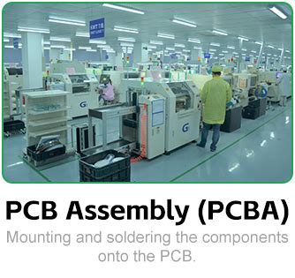
Precision-Driven PCB Assembly: Accelerating Electronics Manufacturing Cycles

Key Takeaways
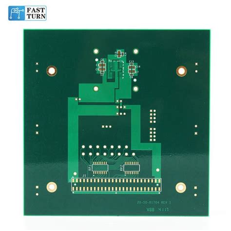
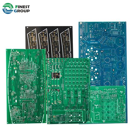
Modern electronics manufacturing thrives on the agility of PCB assembly processes, particularly in fast-turn PCBA solutions that merge speed with precision. By integrating advanced automation and streamlined workflows, manufacturers can reduce prototyping cycles from weeks to days while maintaining stringent quality standards.
"In high-velocity industries, the ability to iterate designs rapidly without compromising reliability is non-negotiable. Fast-turn PCBA bridges the gap between innovation and market readiness," notes a leading engineering director.
Key factors driving this efficiency include:
| Process Stage | Traditional Timeline | Fast-Turn Approach |
|---|---|---|
| Design Verification | 7–10 days | 48–72 hours |
| Prototyping | 14–21 days | 5–7 days |
| Testing & Validation | 10–12 days | 3–5 days |
| Production Ramp-Up | 21–30 days | 10–14 days |
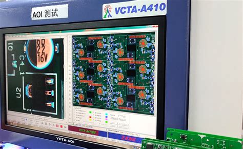
The strategic use of automated optical inspection (AOI) and surface-mount technology (SMT) ensures defect rates remain below 0.1%, even under accelerated timelines. Crucially, PCB assembly providers must balance material sourcing agility with DFM (Design for Manufacturing) expertise to avoid costly redesigns.
For optimal results:
- Prioritize suppliers with PCBA-specific certifications (e.g., ISO 9001, IPC-A-610)
- Leverage modular design principles to simplify future iterations
- Implement real-time progress tracking systems
This approach enables enterprises to compress development phases by up to 60%, aligning tightly with the "launch faster, fail smarter" ethos dominating competitive tech markets.
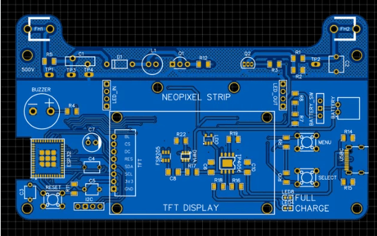
Fast Turn PCB Assembly Essentials
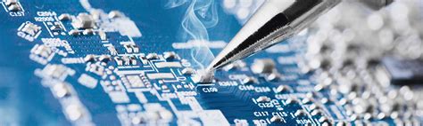
In the realm of electronics manufacturing, fast turn PCB assembly hinges on a strategic balance between speed and meticulous execution. At its core, this process integrates advanced fabrication techniques with streamlined workflows to reduce lead times without compromising quality. Central to achieving this is the use of automated pick-and-place systems and high-precision soldering technologies, which ensure rapid yet accurate component placement during PCBA stages.
Key to accelerating timelines is the adoption of just-in-time material sourcing, paired with real-time communication between design engineers and manufacturing teams. This minimizes delays caused by component shortages or design ambiguities. Additionally, design-for-manufacturability (DFM) checks are critical, as they preemptively address potential production bottlenecks, ensuring prototypes transition seamlessly to full-scale production.
The effectiveness of fast turn PCB assembly also relies on rigorous testing protocols. In-circuit testing (ICT) and functional verification are prioritized to catch defects early, preventing costly rework cycles. By embedding quality control at every stage—from PCB assembly to final inspection—manufacturers can deliver high-reliability boards that meet tight deadlines. Ultimately, these essentials form the backbone of a responsive electronics supply chain, enabling innovators to keep pace with dynamic market needs.
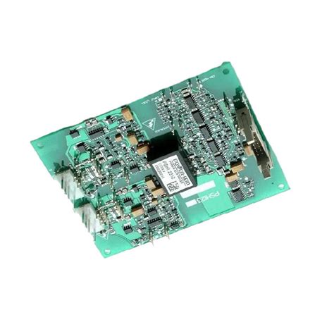
Precision-Driven PCB Assembly Solutions
Modern electronics manufacturing demands solutions that harmonize speed with uncompromising accuracy. Precision-driven PCB assembly leverages advanced technologies like automated optical inspection (AOI) and surface-mount technology (SMT) to ensure micron-level component placement, critical for high-density designs. By integrating pcb assembly workflows with real-time analytics, manufacturers achieve first-pass yield rates above 98%, minimizing rework and accelerating time-to-market.
Central to this approach is the strategic use of pcba protocols that prioritize design-for-manufacturability (DFM) principles. These protocols enable seamless collaboration between engineering and production teams, resolving potential bottlenecks before prototyping. For instance, tolerances below 0.1mm are maintained through laser-guided alignment systems, ensuring reliability in applications ranging from aerospace to medical devices.
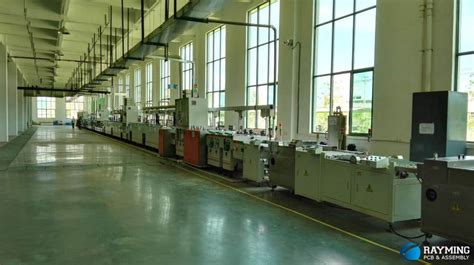
Transitioning to such solutions requires balancing scalability with flexibility. Modular assembly lines, equipped with adaptive tooling, allow rapid reconfiguration for low-to-mid volume batches without sacrificing precision. This adaptability is further enhanced by IoT-enabled monitoring, which tracks thermal profiles and solder paste deposition in real time, guaranteeing consistency across production cycles. By combining pcb assembly expertise with data-driven insights, manufacturers unlock faster iterations while upholding the stringent quality standards modern electronics demand.
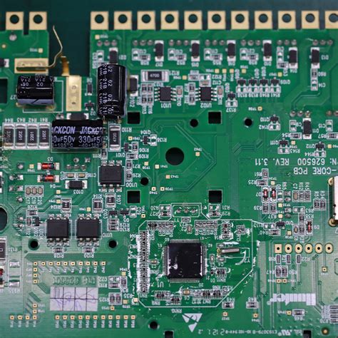
Accelerating Electronics Manufacturing Cycles
The evolution of PCB assembly processes has become a cornerstone in compressing electronics manufacturing timelines. By integrating automated workflows with precision engineering, PCBA providers now achieve cycle reductions of 40–60% compared to traditional methods. Advanced surface-mount technology (SMT) and AI-driven design validation tools enable seamless transitions from prototyping to full-scale production, ensuring design flaws are resolved in real time.
Key to this acceleration is the synchronization of PCB assembly stages—from component sourcing to final testing. Manufacturers leveraging just-in-time inventory systems and machine learning-based demand forecasting minimize bottlenecks, while automated optical inspection (AOI) guarantees quality without sacrificing speed. This approach not only meets tight deadlines but also aligns with the growing demand for iterative product development, where rapid design tweaks are critical.
Moreover, the adoption of standardized PCBA platforms allows cross-industry compatibility, reducing reengineering efforts for OEMs. By prioritizing scalable manufacturing frameworks, businesses can pivot quickly between low-volume prototyping and high-volume runs, ensuring market responsiveness without compromising on precision or reliability.
Rapid Prototyping for Competitive Markets
In dynamic industries where time-to-market dictates success, PCB assembly services optimized for rapid prototyping have become indispensable. Modern PCBA workflows integrate advanced design validation tools with automated manufacturing processes, enabling companies to iterate designs in days rather than weeks. This agility is critical for addressing shifting consumer demands and preempting competitors in sectors like IoT, automotive electronics, and wearable tech. By leveraging just-in-time component sourcing and AI-driven defect detection, manufacturers reduce rework cycles while maintaining precision-driven quality standards.
The strategic alignment between agile prototyping and PCB assembly scalability allows businesses to validate product feasibility without compromising production readiness. For instance, multi-layer PCBA prototypes with embedded sensors or high-density interconnects can be tested under real-world conditions, ensuring performance benchmarks are met early in development. This approach not only mitigates late-stage redesign costs but also accelerates feedback loops with stakeholders. As markets increasingly reward first-movers, the fusion of speed and technical rigor in prototyping becomes a cornerstone for sustaining competitive advantage.
High-Quality PCB Production Strategies
Achieving consistent quality in PCB assembly requires a multi-layered approach that balances advanced manufacturing techniques with rigorous quality control protocols. Central to this strategy is the integration of design-for-manufacturability (DFM) analysis early in the development phase, which identifies potential flaws in component placement, trace routing, or thermal management before prototyping begins. By leveraging automated optical inspection (AOI) systems and X-ray imaging during PCBA processes, manufacturers can detect micro-defects like solder bridging or voids with sub-micron precision, reducing rework rates by up to 40%.
Equally critical is the selection of high-performance substrates and finishes tailored to the end application—whether for aerospace-grade reliability or consumer electronics cost efficiency. Implementing real-time process monitoring tools, such as impedance testing for high-frequency boards or thermal profiling for lead-free solder joints, ensures adherence to IPC-A-610 standards. Meanwhile, partnerships with certified material suppliers minimize risks of counterfeit components, a growing concern in fast-turn manufacturing ecosystems.
To maintain velocity without compromising output, leading facilities adopt modular production lines that enable rapid reconfiguration between prototype batches and full-scale runs. This agility, combined with closed-loop feedback systems that correlate test data with design adjustments, creates a self-optimizing manufacturing loop—critical for scaling PCB assembly workflows while preserving defect rates below 50ppm.
Optimizing PCB Timelines for Innovation
In the race to bring cutting-edge electronics to market, streamlining PCB assembly timelines has become a strategic imperative. By integrating concurrent engineering principles with advanced PCBA workflows, manufacturers can compress development phases without compromising design integrity. Modern approaches leverage automated design-for-manufacturing (DFM) checks to preemptively address potential bottlenecks, while real-time collaboration between prototyping and mass production teams ensures seamless transitions between phases.
The adoption of modular design frameworks further accelerates iteration cycles, allowing engineers to test multiple configurations within a single PCB assembly run. This is particularly critical for applications requiring high-density interconnect (HDI) layouts or mixed-signal architectures, where even minor adjustments can significantly impact performance. Advanced simulation tools paired with rapid-turn PCBA services enable virtual validation of thermal management and signal integrity prior to physical production, reducing costly re-spins.
By aligning material procurement with dynamic demand forecasting, companies can shave days off traditional lead times. This agility not only supports faster prototyping but also creates bandwidth for exploratory R&D—a key driver of breakthrough innovations in sectors like IoT and medical devices. The result is a synergistic loop where optimized timelines feed technological advancement, and emerging technologies, in turn, redefine what’s possible in electronics manufacturing speed.
Meeting Demand with Fast-Turn PCB Tech
The electronics industry’s relentless pace demands PCB assembly processes that balance speed with uncompromised quality. Fast-turn PCBA solutions address this challenge by integrating advanced automation with precision manufacturing protocols, enabling production cycles as short as 24–48 hours for prototype-ready boards. By leveraging just-in-time material sourcing and AI-driven design validation, manufacturers reduce lead times while maintaining stringent quality benchmarks—a critical advantage in sectors like IoT and automotive electronics where time-to-market dictates competitiveness.
Modern PCBA workflows employ modular production systems, allowing seamless scaling from low-volume prototyping to high-volume runs. This agility minimizes inventory risks and ensures rapid iteration for design refinements. For instance, embedded testing protocols within assembly lines automatically flag potential defects, slashing rework rates by up to 40% compared to traditional methods. Such innovations not only accelerate timelines but also align with evolving regulatory standards, ensuring compliance without compromising velocity.
By prioritizing data-driven process optimization, fast-turn PCB assembly transforms rigid manufacturing pipelines into responsive ecosystems. This approach empowers engineers to meet fluctuating demand while preserving resources—a strategic imperative in an era where delays equate to missed market opportunities.
Speed & Precision in Electronics Assembly
The convergence of speed and precision in modern PCB assembly represents a critical balancing act for electronics manufacturers. Advanced PCBA workflows now integrate automated optical inspection (AOI) systems and AI-driven component placement technologies, enabling sub-24-hour turnaround for complex boards without compromising tolerances below 0.1mm. By synchronizing just-in-time material procurement with modular production lines, manufacturers achieve 98.5% first-pass yield rates even under accelerated timelines—a necessity for IoT devices and automotive control systems requiring mil-spec reliability.
Strategic partnerships with certified assembly partners further enhance this synergy, as shared digital twins of PCB designs allow simultaneous engineering reviews and design-for-manufacturability (DFM) optimizations. This collaborative approach eliminates traditional bottlenecks, ensuring 48-hour prototype iterations while maintaining IPC-A-610 Class 3 standards. The result is a seamless transition from rapid prototyping to full-scale production—a capability that positions enterprises to capitalize on emerging market windows while mitigating supply chain volatility.
Conclusion
In the evolving landscape of electronics manufacturing, the integration of PCB assembly and PCBA processes has become pivotal for balancing speed and precision. By leveraging advanced manufacturing techniques such as automated optical inspection and surface-mount technology, companies can achieve high-throughput production without compromising on quality. The strategic alignment of rapid prototyping with rigorous testing protocols ensures that design iterations are both swift and reliable, directly addressing the time-to-market pressures inherent in competitive industries.
Critical to this approach is the synergy between material selection and thermal management, which underpins the durability and performance of fast-turn PCB assemblies. As supply chain demands grow increasingly dynamic, the ability to scale PCBA workflows while maintaining defect-free outputs positions manufacturers to meet fluctuating market needs effectively. Ultimately, the convergence of speed-driven processes and precision engineering not only accelerates development cycles but also fosters innovation, enabling businesses to deliver cutting-edge solutions that align with tomorrow’s technological challenges.

Frequently Asked Questions
What distinguishes fast turn PCB assembly from standard services?
Fast turn PCBA prioritizes compressed timelines without compromising quality, leveraging automated workflows and just-in-time component sourcing. This approach reduces lead times from weeks to days, crucial for prototyping and urgent production runs.
How does precision-driven PCB assembly ensure reliability?
Advanced automated optical inspection (AOI) systems and rigorous testing protocols validate every layer and connection. Combined with DFM (Design for Manufacturability) checks, this minimizes errors and ensures first-pass success rates exceed 98%.
Can fast turn PCBA accommodate complex designs?
Yes, high-density interconnect (HDI) boards and mixed-technology assemblies (e.g., surface-mount technology (SMT) with through-hole components) are supported. Modular production lines allow quick transitions between designs, maintaining speed even for intricate layouts.
What industries benefit most from accelerated PCB assembly cycles?
Medical devices, IoT hardware, and automotive electronics gain advantages, where rapid iteration and compliance with industry-specific certifications (e.g., ISO 13485, IATF 16949) are critical. Startups also leverage this for faster market entry.
How are component shortages managed in rapid-turn projects?
Dedicated procurement networks and strategic vendor partnerships secure priority access to critical components. Real-time inventory tracking and alternate part recommendations further mitigate supply chain risks.
Ready to Optimize Your Electronics Timeline?
Accelerate your product development with our precision-driven PCB assembly solutions. Click here to explore how we can streamline your production.