Precision-Driven PCBA Assembly Techniques for Reliable Electronics

Key Takeaways
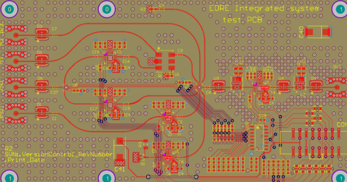
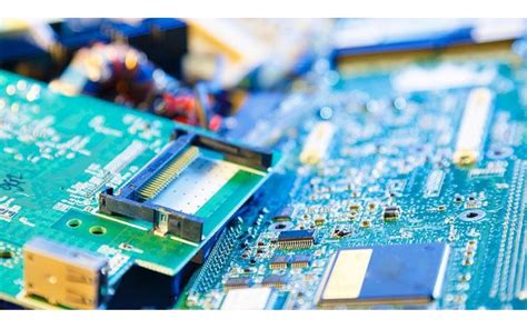
Modern PCBA (Printed Circuit Board Assembly) processes rely on precision-driven methodologies to ensure electronics perform reliably under demanding conditions. Central to this is surface-mount technology (SMT), which enables the placement of miniaturized components with micrometer-level accuracy. By integrating automated optical inspection (AOI) systems, manufacturers can detect defects like soldering anomalies or misalignments early, reducing rework costs and improving yield rates.
"Quality in PCB assembly isn’t just about meeting specifications—it’s about anticipating real-world stressors and designing resilience into every layer."
Critical quality control protocols, such as thermal cycling tests and in-circuit testing (ICT), validate PCBA durability. For instance:
| Technique | Purpose | Impact on Reliability |
|---|---|---|
| Automated X-ray Inspection | Verifies hidden solder joints | Reduces latent defects by 40-60% |
| Functional Testing | Simulates operational environments | Ensures 99.9% post-assembly performance |
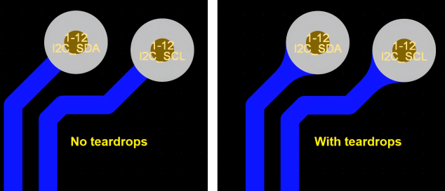
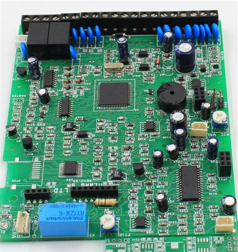
To optimize device reliability, manufacturers prioritize precision PCBA methods, including laser-cut stencils for solder paste application and pick-and-place robotics for component positioning. These strategies, combined with statistical process control (SPC), ensure consistency across high-volume production runs.
Automation further streamlines workflows, minimizing human error while accelerating throughput. For mission-critical applications, rigorous testing standards—such as IPC-A-610 compliance—guarantee that every PCBA meets industry benchmarks for longevity and performance.
Precision-Driven PCBA Assembly for Reliable Electronics
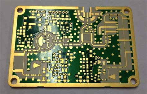
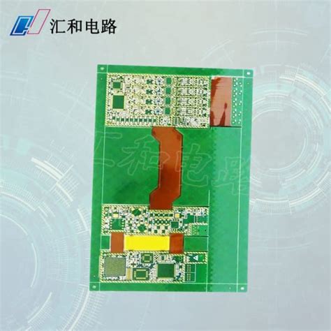
Modern PCB assembly processes rely on precision-driven methodologies to meet the escalating demands for reliability in electronic devices. At the core of PCBA manufacturing lies the integration of micron-level accuracy in component placement, soldering, and substrate alignment. Advanced surface-mount technology (SMT) enables the attachment of miniaturized components, such as 01005 passives or ball grid arrays (BGAs), with tolerances under 50 micrometers. This precision minimizes electrical resistance mismatches and thermal stress points, directly enhancing circuit longevity.
Critical to this approach is the use of automated optical inspection (AOI) systems, which scan solder joints and component orientations at speeds exceeding 20,000 inspections per hour. These systems detect defects like tombstoning or cold joints with 99.98% accuracy, ensuring compliance with IPC-A-610 standards. Additionally, laser-etched fiducial markers guide pick-and-place machines to achieve alignment accuracies within ±25 microns, a necessity for high-density interconnect (HDI) designs.
To further bolster reliability, PCBA workflows incorporate environmentally controlled soldering profiles, optimizing reflow temperatures for lead-free alloys. Such protocols prevent delamination or warping in multilayer boards, particularly in applications exposed to thermal cycling or vibration. By harmonizing precision engineering with rigorous validation, manufacturers deliver PCB assemblies capable of sustaining 100,000+ operational hours in aerospace, medical, and automotive systems—setting the foundation for subsequent discussions on automation and testing innovations.
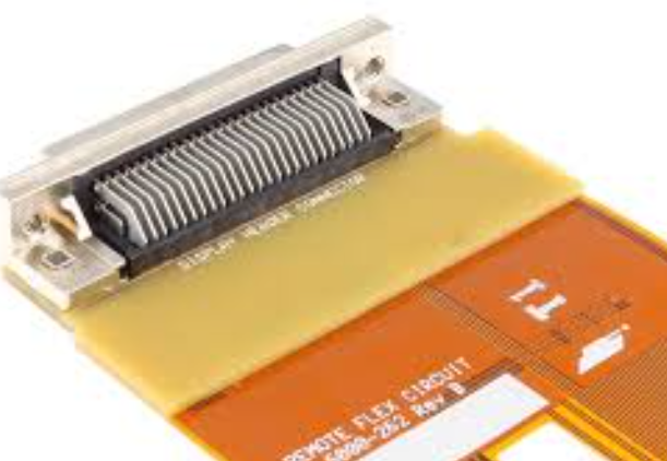
Surface-Mount Technology in Modern PCBA Applications
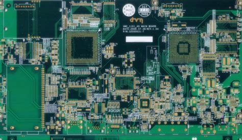
Modern PCB assembly processes rely heavily on surface-mount technology (SMT) to meet the demands of compact, high-performance electronics. Unlike traditional through-hole methods, SMT enables the placement of components directly onto the surface of printed circuit boards (PCBs), significantly reducing size while improving electrical performance. This technique supports the integration of miniature components such as resistors, capacitors, and integrated circuits (ICs), which are critical for devices requiring high-speed operation and minimal footprint.
A key advantage of SMT in PCBA is its compatibility with automated production lines. High-speed pick-and-place machines, combined with precision solder paste application, ensure consistent component alignment and reliable electrical connections. Additionally, reflow soldering—a process where solder paste is melted to form permanent bonds—eliminates manual errors, enhancing overall yield. For industries like telecommunications and medical devices, where thermal management and signal integrity are paramount, SMT provides the necessary precision to maintain performance under demanding conditions.
The scalability of SMT also supports mass production without compromising quality, making it indispensable for modern electronics manufacturing. To explore foundational concepts of PCB design, visit this resource. As devices continue to shrink in size yet grow in complexity, SMT remains central to achieving reliable, high-density PCBA solutions.
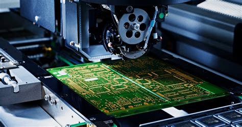
Automated Inspection Systems for Error-Free PCBAs
Modern PCB assembly processes rely on automated inspection systems to eliminate defects and ensure zero-tolerance precision in PCBA manufacturing. These systems integrate advanced imaging technologies, such as automated optical inspection (AOI) and X-ray inspection, to scrutinize solder joints, component placement accuracy, and trace integrity at micron-level resolutions. By replacing error-prone manual checks, automated tools detect flaws like bridging, tombstoning, or misaligned surface-mount devices (SMDs) in real time, reducing rework costs and production delays. Machine learning algorithms further enhance defect recognition, adapting to evolving PCBA designs and complex multilayer layouts. For high-density boards with fine-pitch components, inline inspection systems validate each stage of assembly—from solder paste deposition to final functional testing—ensuring compliance with industry-specific quality benchmarks. This seamless integration of automation not only accelerates throughput but also aligns with stringent quality control protocols, guaranteeing that every PCBA meets performance and reliability standards for mission-critical applications.
Quality Control Protocols Enhancing PCBA Durability
Robust quality control protocols form the backbone of durable PCB assembly processes, ensuring long-term reliability in electronic devices. Modern PCBA manufacturing integrates multi-stage inspections, beginning with automated optical inspection (AOI) systems that detect soldering defects, component misalignment, and trace irregularities. These systems are complemented by X-ray inspection for hidden flaws in ball grid array (BGA) packages or layered substrates. Post-assembly, in-circuit testing (ICT) validates electrical performance by simulating real-world operating conditions, identifying shorts, opens, or impedance mismatches that could compromise functionality.
To further enhance PCBA durability, manufacturers implement environmental stress testing (EST), exposing boards to extreme temperatures, humidity, and vibration. This replicates decades of operational wear within controlled cycles, revealing potential failure points in materials or solder joints. Compliance with IPC-A-610 and IPC-J-STD-001 standards ensures consistency across production batches, while traceability systems track defects back to specific process stages for corrective action. By combining these protocols, PCB assembly achieves the precision required for mission-critical applications, from medical devices to aerospace systems, where zero-failure tolerance is non-negotiable.
Advanced Techniques for High-Performance Electronics Assembly
Modern PCBA manufacturing demands cutting-edge methodologies to meet the rigorous performance requirements of today’s electronics. Central to this is the integration of precision-driven PCB assembly processes, which combine high-accuracy placement systems with advanced soldering techniques. For instance, surface-mount technology (SMT) enables the placement of microcomponents at speeds exceeding 50,000 parts per hour, minimizing human error while maximizing throughput.
Automated optical inspection (AOI) and X-ray systems further ensure defect-free PCBA by detecting micro-cracks, solder bridging, or misaligned components at resolutions down to 10 microns. These systems work in tandem with AI-powered analytics to predict potential failures before they compromise device reliability. Another critical element is the use of lead-free soldering alloys, which enhance thermal stability and compliance with global environmental standards.
To maintain consistency, manufacturers are adopting closed-loop feedback systems that adjust parameters like reflow oven temperatures in real time. This approach reduces thermal stress on sensitive components, a key factor in extending the lifespan of high-density PCB assemblies. For deeper insights into evolving PCB assembly trends, industry experts highlight innovations such as additive manufacturing for flexible circuits and embedded component technologies.
By harmonizing these techniques, PCBA providers achieve not only superior electrical performance but also the durability required for applications ranging from medical devices to aerospace systems.
Optimizing Device Reliability Through Precision PCBA Methods
Achieving consistent reliability in electronic devices hinges on precision-driven methodologies within PCB assembly processes. By integrating high-accuracy placement systems and temperature-controlled soldering techniques, manufacturers minimize defects such as solder bridging or component misalignment, which compromise PCBA integrity. Advanced tools like laset-aligned pick-and-place machines ensure micron-level accuracy, particularly critical for miniaturized components in IoT or medical devices.
A cornerstone of reliability lies in automated optical inspection (AOI) systems, which scan PCBAs for microscopic flaws undetectable by manual checks. Pairing AOI with X-ray inspection further validates hidden connections, such as ball grid arrays (BGAs), ensuring structural soundness. Additionally, statistical process control (SPC) monitors production variables in real time, enabling immediate corrections to deviations that could affect long-term performance.
Material selection also plays a pivotal role. Utilizing low-voiding solder pastes and high-Tg substrates reduces thermal stress during operation, extending the lifespan of PCB assemblies. By harmonizing these precision methods with rigorous testing protocols—such as thermal cycling and vibration tests—manufacturers elevate PCBA durability, meeting stringent demands for aerospace, automotive, and industrial applications. This multi-layered approach ensures devices withstand operational extremes while maintaining functional consistency over time.
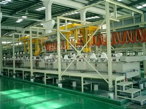
The Role of Automation in Streamlined PCBA Production
Automation has become the backbone of modern PCB assembly processes, enabling manufacturers to achieve unprecedented speed and consistency in PCBA production. Advanced robotic systems, such as pick-and-place machines, execute micron-level component positioning with minimal human intervention, significantly reducing assembly errors. These systems integrate seamlessly with automated optical inspection (AOI) tools, which scan boards for defects like misaligned solder joints or missing components, ensuring adherence to stringent quality benchmarks.
A critical advantage of automation lies in its ability to scale production while maintaining uniformity. For instance, reflow soldering ovens equipped with precise temperature profiles optimize solder joint integrity across high-volume batches. Furthermore, automated workflows support panelization strategies, where multiple PCBA units are processed simultaneously on a single panel, minimizing material waste and maximizing throughput.
By eliminating manual handling variability, automation not only accelerates time-to-market but also enhances long-term reliability in electronic devices. This alignment of efficiency and precision underscores its indispensable role in meeting the demands of today’s fast-paced, quality-driven electronics industry.
Ensuring Longevity with Rigorous PCBA Testing Standards
To guarantee the durability of electronic devices, PCBA manufacturers implement multilayered testing protocols that validate performance under real-world conditions. PCB assembly processes integrate environmental stress testing (EST) to simulate extreme temperatures, humidity, and mechanical shocks, ensuring boards withstand operational challenges. Advanced thermal cycling exposes assemblies to rapid temperature fluctuations, identifying potential solder joint weaknesses before deployment.
Automated electrical testing verifies circuit functionality, detecting shorts, opens, or impedance mismatches that could compromise reliability. In-circuit testing (ICT) and functional testing (FCT) are prioritized to assess both individual components and full-system behavior. For high-density PCBA designs, X-ray inspection supplements visual checks to scrutinize hidden connections, such as ball grid arrays (BGAs), ensuring solder integrity.
Compliance with industry standards like IPC-A-610 and ISO-9001 further reinforces quality, mandating strict criteria for solder quality, component placement, and cleanliness. By combining predictive analytics with failure mode analysis, manufacturers proactively address wear patterns, extending product lifespans. These rigorous testing frameworks not only reduce field failures but also align with evolving demands for electronics that deliver consistent performance across years of use.
Conclusion
The evolution of PCB assembly processes underscores the critical role of precision in manufacturing reliable electronic systems. By integrating surface-mount technology (SMT) and automated optical inspection (AOI) systems, modern PCBA workflows achieve unprecedented accuracy, minimizing defects and ensuring consistent performance. These advancements, paired with statistical process control (SPC) methodologies, enable manufacturers to preemptively address potential failures, extending the lifespan of end products.
As industries demand higher functionality in compact designs, PCB assembly techniques must prioritize both miniaturization and durability. Thermal management strategies and conformal coating applications further enhance resilience against environmental stressors, a necessity for applications in aerospace, medical devices, and IoT ecosystems. For organizations seeking scalable solutions, partnering with experts in advanced PCBA production ensures alignment with evolving technological standards.
Ultimately, the synergy between precision engineering and rigorous testing protocols defines the success of contemporary electronics. By adopting these PCBA best practices, manufacturers not only meet current market demands but also future-proof their innovations against emerging challenges.
Frequently Asked Questions
What distinguishes PCB assembly from PCBA?
PCB assembly refers to the process of populating a bare circuit board with components, while PCBA (Printed Circuit Board Assembly) denotes the completed board with all electronic parts mounted and ready for integration. The distinction lies in the completion stage—PCBA implies a fully functional unit post-assembly.
How does surface-mount technology improve PCBA reliability?
Surface-mount technology (SMT) enables smaller component placements and higher circuit density, reducing signal loss and mechanical stress. This precision minimizes soldering defects, enhancing PCBA durability in compact, high-performance devices like wearables or IoT sensors.
Why are automated inspection systems critical in PCB assembly?
Automated optical inspection (AOI) and X-ray testing detect microscopic flaws—such as misaligned components or insufficient solder—that manual checks might miss. These systems ensure 99.9% defect-free PCBAs, aligning with stringent quality benchmarks for aerospace or medical electronics.
What quality control protocols ensure long-term PCBA performance?
Thermal cycling tests, environmental stress screening (ESS), and conformal coating applications validate PCBA resilience against humidity, temperature fluctuations, and vibration. Combined with traceability systems, these protocols guarantee compliance with ISO 9001 and IPC-A-610 standards.
How does automation accelerate PCB assembly timelines?
Robotic pick-and-place machines and AI-driven solder paste dispensers achieve 50% faster throughput than manual methods. Automated workflows also reduce human error, ensuring consistent PCBA quality for high-volume orders in automotive or industrial sectors.
Ready to Optimize Your Next PCBA Project?
For tailored PCB assembly solutions that prioritize precision and reliability, please click here to explore our advanced manufacturing capabilities.