Precision-Driven PCBA Manufacturing for Superior Reliability

Key Takeaways
Achieving reliable PCBA outcomes hinges on integrating precision-driven methodologies across design, PCB assembly, and testing phases. Central to this approach is the strategic use of automated assembly systems, which minimize human error while ensuring consistent solder joint quality and component placement accuracy. Mission-critical applications demand adherence to rigorous quality protocols, including automated optical inspection (AOI) and X-ray verification, to detect microfractures or misalignments invisible to the naked eye.
Equally vital is the optimization of material selection, where substrate thermal stability and solder alloy composition directly impact PCBA longevity under extreme operational stresses. Advanced manufacturers employ failure mode analysis to refine material pairings, balancing electrical performance with environmental resilience. By aligning PCB assembly workflows with industry-certified standards (e.g., IPC-A-610), stakeholders ensure compliance while streamlining scalability for high-volume production.
Transitioning to these practices requires cross-functional collaboration between design engineers and PCBA specialists, fostering innovations like embedded testing protocols and predictive maintenance algorithms. This synergy not only elevates reliability but also reduces time-to-market for electronics reliant on zero-defect operation throughout their product lifecycle.

Automating PCBA for Reliability
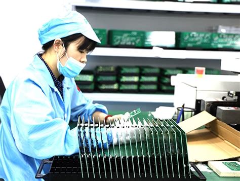
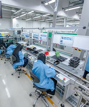
Modern PCBA processes increasingly rely on automation to eliminate human error and ensure consistent performance in mission-critical applications. By integrating robotic PCB assembly systems—such as automated pick-and-place machines and soldering robots—manufacturers achieve micron-level accuracy in component placement, reducing defects like misalignment or cold joints. Advanced optical inspection (AOI) systems further enhance reliability by scanning boards at high resolution to detect anomalies invisible to the human eye. This zero-defect mindset is critical for industries like aerospace and medical devices, where even minor flaws can compromise system integrity.
Automation also streamlines traceability, with digital workflows tracking every stage of PCBA production. Real-time data analytics enable rapid adjustments, ensuring compliance with stringent industry standards. For example, failure mode and effects analysis (FMEA) is often embedded into automated processes to preemptively address potential failure points. Such proactive measures not only improve yield rates but also extend the lifecycle of electronic assemblies. By prioritizing automation, manufacturers balance speed and precision, delivering PCB assembly solutions that meet the escalating demands for reliability in today’s interconnected technologies.

Rigorous PCBA Quality Control
Modern PCBA processes demand meticulous quality assurance frameworks to prevent defects in mission-critical electronics. At the core of rigorous PCB assembly quality control lies a multi-layered inspection system combining automated optical inspection (AOI), X-ray imaging, and in-circuit testing (ICT). These technologies work synergistically to identify issues like solder bridging, component misalignment, or micro-cracks invisible to the naked eye.
"A single undetected fault in PCBA can cascade into system failures costing 10x more post-deployment," notes Dr. Elena Voss, a quality assurance specialist at OES-EMS.
Below is a comparison of key inspection methods:
| Method | Purpose | Defect Detection Rate |
|---|---|---|
| AOI | Surface-level component analysis | 98.5% |
| X-ray Imaging | Subsurface solder joint analysis | 99.2% |
| ICT | Electrical functionality verification | 97.8% |
To ensure consistency, leading manufacturers implement statistical process control (SPC), tracking variables like solder paste viscosity and reflow oven temperature in real time. Material integrity is further validated through thermal cycling tests and vibration resistance evaluations, critical for aerospace or automotive applications.
Pro Tip: Always verify that your PCB assembly partner maintains ISO 9001 and IPC-A-610 certifications—non-negotiable benchmarks for defect-per-million (DPM) thresholds below 50.
While automated systems handle 85% of defect detection, manual cross-checks by certified technicians remain vital for complex assemblies. This hybrid approach reduces false negatives by 22% compared to fully automated workflows, according to 2023 industry benchmarks.
Transitioning seamlessly to material optimization, rigorous quality protocols inherently depend on selecting components rated for operational stress profiles—a bridge to the next phase of PCBA excellence.

Optimizing PCBA Material Selection
At the core of high-reliability PCBA manufacturing lies the strategic selection of materials, a process that directly impacts electrical performance, thermal management, and long-term durability. Substrate composition, solder mask quality, and conductive material properties must align with the operational demands of the end application. For mission-critical electronics, engineers prioritize substrates with low coefficient of thermal expansion (CTE) to minimize stress during thermal cycling, paired with high-glass-transition-temperature (Tg) laminates for stability in elevated temperatures.
The choice of PCB assembly materials extends beyond base layers—solder alloys, conformal coatings, and surface finishes require meticulous evaluation. Lead-free solder formulations, for instance, balance environmental compliance with mechanical strength, while silver-based finishes enhance conductivity in high-frequency applications. Advanced PCBA workflows leverage material databases and simulation tools to predict interactions between components and substrates, ensuring compatibility under extreme conditions like vibration or humidity.
Rigorous adherence to industry standards (e.g., IPC-4101 for laminates) further refines material optimization. By correlating failure mode analysis with real-world performance data, manufacturers systematically eliminate weak points, achieving PCBA designs that meet both functional requirements and lifecycle expectations. This precision-driven approach ensures every material layer contributes to the assembly’s resilience, forming the foundation for subsequent quality control and testing phases.

Precision-Driven PCBA Engineering
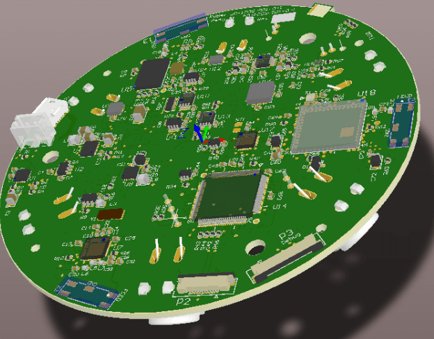
At the heart of PCBA reliability lies precision engineering, which harmonizes design intent with manufacturing execution. Advanced PCB assembly processes leverage high-accuracy component placement systems, often achieving tolerances below 0.1mm, to ensure flawless electrical connectivity. Sophisticated soldering techniques, such as reflow profiling with nitrogen-enriched environments, minimize voids and thermal stress in mission-critical boards. Engineers employ design for manufacturability (DFM) principles to preemptively address potential issues like solder bridging or component misalignment, while automated optical inspection (AOI) systems validate alignment accuracy at micron-level resolutions.
Furthermore, precision-driven workflows integrate real-time feedback loops between PCBA prototyping and mass production, enabling rapid adjustments to material thicknesses or trace widths. This approach optimizes signal integrity in high-frequency applications and mitigates electromagnetic interference (EMI) risks. By balancing thermal management requirements with spatial constraints, engineers ensure consistent performance across operating temperatures ranging from -40°C to 125°C. Such meticulous attention to geometric and electrical tolerances directly translates to enhanced product longevity, particularly in aerospace, medical, and industrial automation systems where component-level precision dictates system-wide reliability.

Mission-Critical PCBA Standards
In industries where system failures can lead to catastrophic outcomes—such as aerospace, defense, and medical devices—adherence to mission-critical PCBA standards is non-negotiable. These frameworks mandate stringent requirements for PCB assembly processes, ensuring every PCBA meets exacting performance benchmarks. Central to these standards is the integration of traceability protocols, which track components from procurement to final testing, minimizing risks of counterfeit parts or material inconsistencies.
Key criteria include compliance with IPC-610 and IPC-J-STD-001 specifications, which define acceptability for soldering, component placement, and electrical performance. For instance, thermal cycling and vibration resistance tests validate PCBA durability under extreme conditions, while electromagnetic compatibility (EMC) assessments ensure interference-free operation in dense electronic ecosystems. Manufacturers must also align with industry-specific certifications like AS9100D (aerospace) or ISO 13485 (medical devices), reinforcing accountability across supply chains.
To maintain alignment with these standards, automated optical inspection (AOI) and X-ray testing are deployed to detect micro-scale defects invisible to manual checks. By harmonizing rigorous validation processes with advanced manufacturing technologies, PCB assembly providers guarantee that mission-critical systems operate with zero tolerance for error, safeguarding both functionality and human safety.
Advanced Testing for PCBA Reliability
Modern PCBA manufacturing relies on multilayered testing methodologies to ensure mission-critical performance in demanding environments. At the core of these protocols is automated optical inspection (AOI), which scans solder joints, component placement, and circuitry for microscopic defects at speeds surpassing manual checks. Complementing AOI, X-ray inspection penetrates layered boards to verify BGA (ball grid array) connections and internal via integrity—critical for high-density designs. Environmental stress testing, including thermal cycling and humidity exposure, simulates real-world operating conditions to identify failure points before deployment.
For PCB assembly destined for aerospace or medical applications, in-circuit testing (ICT) validates electrical functionality by probing individual nodes, while functional testing assesses the entire board’s behavior under simulated workloads. Advanced systems integrate machine learning algorithms to analyze historical defect data, refining inspection criteria dynamically. By coupling these techniques with IPC-A-610 standards compliance, manufacturers achieve near-zero defect rates, extending product lifecycles and minimizing field failures. This rigorous approach ensures PCBA reliability aligns with the precision demands of modern electronics.
PCBA Best Practices for Electronics
Implementing PCBA best practices requires balancing design precision with manufacturing rigor to achieve consistent performance in electronic systems. Central to this approach is integrating PCB assembly processes with design for manufacturability (DFM) principles, ensuring layouts account for thermal dynamics, signal integrity, and component density. For instance, optimizing pad geometries and solder mask alignments during PCBA design minimizes defects like bridging or tombstoning, particularly in high-density interconnect (HDI) boards.
Equally critical is aligning PCB assembly workflows with industry-recognized standards, such as IPC-A-610, to govern solder joint quality and component placement accuracy. Automated optical inspection (AOI) and X-ray testing further validate assembly integrity, flagging microscopic flaws that could compromise reliability in mission-critical applications. Additionally, adopting traceability systems ensures component provenance and process accountability, which is vital for sectors like aerospace or medical electronics.
Material selection also intersects with PCBA best practices, as substrates and solder alloys must align with operational stressors, such as thermal cycling or vibration. For example, high-Tg laminates enhance thermal resilience, while low-void solder pastes improve electrical continuity. By harmonizing these elements—advanced automation, stringent quality checks, and material science—manufacturers can deliver PCBA solutions that meet both functional demands and long-term reliability expectations.
Material Optimization in PCBAs
The foundation of reliable PCBA lies in strategic material selection, where every component’s properties directly influence performance in mission-critical environments. PCB assembly processes demand substrates, laminates, and solders engineered for thermal stability, electrical conductivity, and mechanical resilience. For instance, high-frequency applications prioritize low-loss dielectric materials to minimize signal distortion, while industrial-grade assemblies require flame-retardant laminates to meet safety standards.
Advanced alloys, such as lead-free solder with silver additives, enhance joint durability under thermal cycling, reducing failure risks in harsh operating conditions. Similarly, copper weights and finishes are optimized to balance current-carrying capacity with signal integrity. Material compatibility with automated PCBA workflows is equally critical—components must withstand reflow temperatures without warping or delamination.
Quality-driven manufacturers employ cross-sectional analysis and accelerated life testing to validate material choices, ensuring alignment with PCB assembly requirements. By integrating data-driven insights into material optimization, engineers achieve a harmonized balance between cost-efficiency and long-term reliability, reinforcing the backbone of precision-driven electronics manufacturing.
Conclusion
As the final stage of production, precision-driven PCBA manufacturing ensures that mission-critical electronics meet the highest standards of reliability. By integrating advanced automation with rigorous quality protocols, manufacturers achieve consistent results across PCB assembly workflows. This approach minimizes human error while optimizing traceability, particularly for high-complexity boards requiring micron-level accuracy.
The selection of high-performance materials—from thermally stable substrates to lead-free solder alloys—plays a pivotal role in enhancing the durability of PCBA-integrated systems. When combined with industry-leading standards, these practices ensure compliance with stringent environmental and operational requirements. Advanced testing methodologies, such as automated optical inspection (AOI) and in-circuit testing (ICT), further validate the integrity of assembled boards under simulated stress conditions.
Ultimately, the convergence of precision engineering and data-driven process control elevates PCB assembly from a routine task to a strategic asset. Manufacturers prioritizing these principles not only mitigate field failure risks but also future-proof their designs against evolving technological demands. The result is a seamless alignment between PCBA reliability and the performance thresholds of next-generation electronic systems.
FAQs
How does automation enhance reliability in PCB assembly?
Advanced automation in PCBA minimizes human error through robotic placement of components and AI-driven inspection systems. This ensures consistent solder joint quality and reduces defects in high-volume production.
What quality control measures are critical for mission-critical electronics?
Rigorous PCBA testing protocols, including automated optical inspection (AOI), X-ray analysis, and thermal cycling, validate performance under extreme conditions. These steps ensure compliance with IPC-A-610 and J-STD-001 standards for reliability.
Why is material selection pivotal in PCB assembly?
Optimal materials, such as high-Tg laminates and low-loss dielectrics, prevent delamination and signal degradation. Proper selection directly impacts thermal stability and longevity, especially in high-frequency or high-power applications.
How does precision engineering address challenges in PCBA for aerospace?
Tight tolerance controls, microvia drilling, and impedance matching ensure signal integrity in compact, vibration-prone environments. This precision is vital for mission-critical systems requiring zero failure rates.
What best practices extend the lifecycle of industrial electronics?
Implementing conformal coating, optimizing trace routing for heat dissipation, and using moisture-resistant substrates enhance durability. Regular design-for-manufacturability (DFM) reviews further mitigate risks in PCB assembly.
Ready to Optimize Your PCBA Workflow?
For tailored solutions in precision-driven PCB assembly, please click here to explore our advanced manufacturing capabilities.