Precision Engineering in PCB Production and Assembly
Key Takeaways
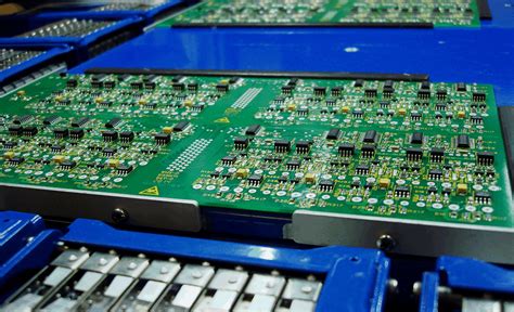
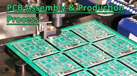
Modern PCB assembly processes rely on precision engineering to balance speed, accuracy, and reliability. Central to this is automated component integration, which minimizes human error while enabling high-volume production. Techniques such as surface-mount technology (SMT) and automated optical inspection (AOI) ensure components are placed and soldered with micron-level accuracy. For PCBA (printed circuit board assembly), design for manufacturability (DFM) checks optimize layouts for seamless integration with robotic systems.
Tip: Always validate design files with thermal simulation tools before production to identify potential soldering defects or heat dissipation issues.
Rigorous quality control standards, including in-circuit testing (ICT) and functional testing, verify electrical performance and durability. Advanced PCB production workflows now incorporate machine learning algorithms to predict and correct assembly anomalies in real time. Additionally, selecting high-performance substrates and low-loss dielectrics directly impacts signal integrity, especially in high-frequency applications.
"Automation isn’t just about speed—it’s about consistency. Even minor deviations in component placement can cascade into system failures."
By harmonizing PCB assembly automation with precision engineering principles, manufacturers achieve tighter tolerances and higher yields. This synergy is critical for industries like aerospace and medical devices, where microelectronics manufacturing demands zero-defect outcomes.
Precision Engineering in PCB Manufacturing
Precision engineering forms the backbone of modern PCB assembly processes, ensuring the seamless integration of complex circuits into compact designs. At its core, this discipline leverages laser-direct imaging (LDI) and automated optical inspection (AOI) systems to achieve micron-level accuracy in trace routing and via formation. These technologies minimize human error while enabling the production of high-density interconnect (HDI) boards, critical for applications like IoT devices and aerospace systems.
A key aspect of precision manufacturing lies in material selection. Advanced substrates, such as polyimide-flexible laminates or low-loss dielectrics, are paired with ultra-fine soldering pastes to maintain signal integrity under extreme conditions. For PCBA workflows, robotic pick-and-place machines equipped with machine vision ensure components as small as 01005 packages are positioned within ±25µm tolerances.
| Process Stage | Precision Metric | Industry Standard |
|---|---|---|
| Drilling | Hole Diameter | ±20µm |
| Etching | Trace Width | ±10µm |
| Solder Mask | Alignment | ±15µm |
To sustain consistency, real-time monitoring systems track variables like reflow oven temperature gradients and stencil pressure during solder paste application. This data-driven approach not only enhances yield rates but also aligns with PCB assembly quality benchmarks such as IPC-A-610 and J-STD-001. By harmonizing cutting-edge machinery with rigorous process controls, manufacturers achieve the reliability demanded by today’s high-frequency and miniaturized electronics.
Automated Component Integration Techniques
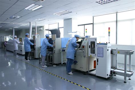
Modern PCB assembly processes rely heavily on automated component integration to achieve the speed and accuracy demanded by today’s microelectronics industry. PCBA (Printed Circuit Board Assembly) systems utilize robotic pick-and-place machines equipped with high-resolution vision systems to position surface-mount devices (SMDs) with micron-level precision. These systems integrate advanced algorithms to map component placement, ensuring alignment with design specifications while minimizing human error.
A critical advancement in this field is the adoption of automated optical inspection (AOI), which scans boards post-placement to detect misalignments or soldering defects. Combined with solder paste printers that apply adhesives uniformly, these technologies enable seamless transitions between assembly stages. For high-density designs, laser-assisted calibration further refines placement accuracy, particularly for fine-pitch components like BGAs or QFNs.
By leveraging PCB assembly automation, manufacturers achieve consistent throughput while adhering to thermal management protocols during reflow soldering. This ensures components withstand operational stresses without compromising electrical integrity. Additionally, PCBA workflows now incorporate real-time data analytics, allowing engineers to optimize machine performance and adapt to evolving design complexities. Such integration not only accelerates production but also aligns with the rigorous quality control standards discussed in subsequent sections of this article.
Quality Control Standards for PCB Assembly
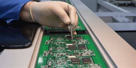
Maintaining stringent quality control standards is critical in PCB assembly to ensure the reliability and functionality of electronic devices. Modern PCBA workflows incorporate automated optical inspection (AOI) systems, which scan boards for defects like misaligned components or solder bridging. These systems are complemented by X-ray inspection for verifying hidden connections in multilayer designs, such as ball grid array (BGA) soldering integrity.
Material verification is equally vital, with suppliers required to adhere to IPC-A-610 and IPC-J-STD-001 specifications for solderability and component placement. Statistical process control (SPC) methods track production metrics in real time, enabling rapid adjustments to minimize deviations. For high-reliability applications, environmental stress testing—including thermal cycling and vibration tests—validates performance under extreme conditions.
A key focus in PCBA quality assurance lies in supply chain traceability, ensuring components meet anti-counterfeiting protocols. Advanced facilities also employ in-circuit testing (ICT) and functional testing to validate electrical behavior against design parameters. By integrating these protocols, manufacturers reduce failure rates while aligning with industry benchmarks for zero-defect manufacturing. This systematic approach not only safeguards product longevity but also supports seamless transitions into downstream design optimization phases.
Optimizing Circuit Performance Through Design
At the core of high-performance electronics lies strategic design optimization, where PCB assembly outcomes are directly influenced by layout decisions. Engineers prioritize signal integrity through controlled impedance routing and minimize electromagnetic interference (EMI) by optimizing component placement. Advanced simulation tools, such as SPICE models and electromagnetic field solvers, enable precise prediction of circuit behavior before prototyping. Implementing Design for Manufacturing (DFM) principles ensures compatibility with automated PCBA processes, reducing defects during high-volume production. Thermal management strategies, including copper pours and via arrays, prevent localized overheating in densely packed designs. Material selection—such as high-frequency laminates for RF applications—further enhances performance by minimizing dielectric losses. By integrating Design for Testing (DFT) features like test points, manufacturers maintain quality control without compromising board real estate. These methodologies collectively elevate end-product reliability while streamlining the transition from design to functional assembled PCB systems.
Advanced PCB Production Process Innovations
The evolution of PCB assembly technologies has introduced groundbreaking methodologies to enhance manufacturing precision and efficiency. Modern PCBA workflows now integrate laser-direct imaging (LDI) systems, which eliminate photomasks to achieve micron-level accuracy in circuit patterning. This innovation reduces material waste and accelerates prototyping cycles, particularly for high-density interconnect (HDI) designs. Additionally, additive manufacturing techniques, such as aerosol jet printing, enable the deposition of conductive inks onto complex substrates, expanding possibilities for flexible and hybrid electronics.
Automation remains central to advancing PCB assembly, with robotic pick-and-place systems achieving placement speeds exceeding 25,000 components per hour. These systems leverage machine vision and AI-driven algorithms to ensure precise alignment, even for ultra-fine-pitch components. Concurrently, in-line inspection tools, like automated optical inspection (AOI), validate solder joint integrity and component orientation in real time, minimizing defects during PCBA. Innovations in thermal management—such as embedded copper pillars and advanced via-filling—further optimize heat dissipation in multilayer boards, critical for high-power applications. By harmonizing these advancements, manufacturers achieve shorter lead times while maintaining the stringent tolerances demanded by aerospace, medical, and IoT industries.
Ensuring Reliability in Electronic Assemblies
Achieving dependable performance in PCB assembly requires a combination of advanced manufacturing protocols and systematic validation processes. At the core of reliable electronic assemblies lies the integration of automated optical inspection (AOI) and X-ray testing, which identify defects like soldering voids or misaligned components during PCBA stages. These tools ensure microscopic precision, critical for high-density interconnect (HDI) boards used in aerospace or medical devices.
Material selection further bolsters reliability, with thermal-resistant substrates and lead-free solder alloys minimizing failure risks under extreme operating conditions. For PCB assembly workflows, in-circuit testing (ICT) validates electrical functionality, while environmental stress screening (ESS) simulates real-world scenarios to expose latent flaws. Modern PCBA lines also leverage predictive analytics to monitor process variables, such as reflow oven temperature profiles, ensuring consistent solder joint quality.
Transitioning from design to production, collaboration between engineers and manufacturers ensures adherence to IPC-A-610 standards, which define acceptability criteria for electronic assemblies. By combining rigorous testing, robust materials, and data-driven process control, manufacturers mitigate risks of field failures, extending the lifecycle of mission-critical systems. This holistic approach aligns with evolving industry demands for miniaturization and higher operational tolerances in PCB assembly workflows.
PCB Assembly Automation Best Practices
Implementing PCB assembly automation requires strategic integration of technology and process design to maximize efficiency while maintaining precision. Modern automated component placement systems leverage PCBA-optimized workflows, combining high-speed pick-and-place machines with vision-guided robotics to achieve micron-level accuracy. These systems reduce human error by 60–80% compared to manual assembly, particularly when handling miniaturized components like 01005 passives or micro-BGA packages.
Critical to success is aligning PCB assembly parameters with design-for-manufacturability (DFM) principles. Automated optical inspection (AOI) systems, paired with real-time feedback loops, ensure solder joint integrity and component alignment during PCBA processes. For example, inline 3D SPI (solder paste inspection) tools preemptively flag deviations in paste volume, preventing defects before reflow stages.
Transitioning to automation also demands robust traceability protocols. Barcode/RFID tracking integrated with enterprise resource planning (ERP) systems enables full lifecycle monitoring of PCB assembly batches. This becomes vital in industries like medical or aerospace, where compliance with IPC-A-610 Class 3 standards is non-negotiable.
Finally, balancing speed with flexibility remains key. Modular PCBA lines that adapt to mixed-product environments—using programmable logic controllers (PLCs) and adaptive feeders—support rapid changeovers without sacrificing throughput. By embedding machine learning algorithms, these systems progressively optimize placement sequences, cutting cycle times by 12–18% per production iteration.
Microelectronics Manufacturing Precision Methods
Achieving micrometer-level accuracy in PCB assembly requires integrating advanced manufacturing techniques with cutting-edge automation. Modern microelectronics fabrication employs photolithography and laser direct imaging (LDI) to etch circuit patterns with tolerances below 10µm, ensuring consistent signal integrity across high-density interconnects (HDIs). For PCBA processes, automated optical inspection (AOI) systems and X-ray tomography verify solder joint quality, detecting voids or misalignments invisible to the human eye.
Precision extends to component placement, where robotic pick-and-place machines achieve placement accuracies of ±25µm, critical for miniaturized designs. Thermal management techniques, such as controlled reflow soldering profiles, prevent warping or delamination during PCB assembly, maintaining structural stability. Additionally, embedded passive components and 3D-printed conductive traces enable tighter integration, reducing parasitic effects that degrade circuit performance.
To sustain precision, manufacturers adopt statistical process control (SPC), analyzing real-time data from production lines to adjust parameters like solder paste viscosity or stencil pressure. These methods, combined with adherence to IPC-A-610 and IPC-J-STD-001 standards, ensure PCBA outputs meet aerospace and medical-grade reliability requirements. By harmonizing advanced machinery with rigorous protocols, the industry continues to push the boundaries of miniaturization and functional density in electronic systems.
Conclusion
The evolution of PCB production and assembly reflects the growing demand for high-density, high-reliability electronics across industries. By integrating automated component placement systems and advanced inspection protocols, manufacturers achieve pcb assembly processes that minimize human error while maximizing throughput. The transition to pcba (Printed Circuit Board Assembly) solutions underscores the importance of harmonizing design intent with manufacturing precision, particularly in applications requiring microelectronics-grade accuracy.
As the industry shifts toward smart manufacturing, innovations in pcb assembly workflows—from solder paste inspection to automated optical alignment—ensure consistent adherence to sub-10μm tolerance thresholds. These advancements, coupled with pcba-specific quality frameworks like IPC-A-610 and J-STD-001, solidify the foundation for zero-defect manufacturing. Ultimately, the synergy between precision engineering and scalable automation in pcb production and assembly not only elevates circuit performance but also future-proofs electronic systems against evolving technical demands.
Frequently Asked Questions
What distinguishes standard PCB assembly from PCBA?
PCB assembly refers to the process of populating a bare circuit board with components, while PCBA (Printed Circuit Board Assembly) denotes the completed, functional board after soldering and testing. The latter includes rigorous validation to meet performance and reliability benchmarks.
How does precision engineering enhance PCB assembly quality?
Advanced techniques like laser-aligned placement and automated optical inspection (AOI) ensure micron-level accuracy in component positioning. These methods minimize human error, enabling consistent PCBA outcomes even for high-density designs.
What quality control measures are critical in PCB assembly?
Key steps include in-circuit testing (ICT), functional testing, and X-ray inspection for hidden solder joints. Automated systems flag defects like shorts or misalignments, ensuring compliance with industry standards such as IPC-A-610.
Why is automation vital in modern PCBA workflows?
Automation accelerates throughput while maintaining repeatability across large batches. Pick-and-place machines, for instance, achieve speeds of 30,000 components per hour, reducing lead times without compromising precision engineering principles.
What factors affect the reliability of PCB assemblies in harsh environments?
Materials like high-Tg substrates and conformal coatings protect against thermal stress and moisture. Additionally, PCBA designs incorporating redundancy and robust trace routing improve resilience in extreme conditions.
How do designers optimize PCB assemblies for signal integrity?
Techniques include impedance matching, ground plane optimization, and minimizing via stubs. Simulation tools predict electromagnetic interference (EMI) risks early, ensuring circuit performance aligns with design specifications.
Explore Custom PCB Assembly Solutions Today
For tailored PCBA services that prioritize precision and reliability, please click here to consult with our engineering team.