Precision Engineering: Streamlining PCB Assembly for Optimal Performance

Key Takeaways
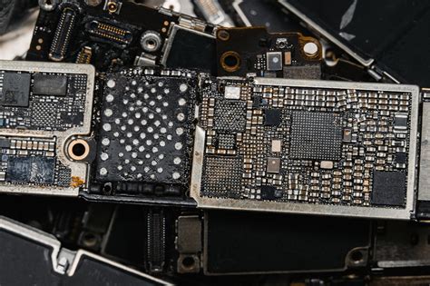
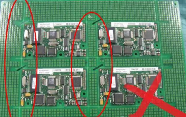
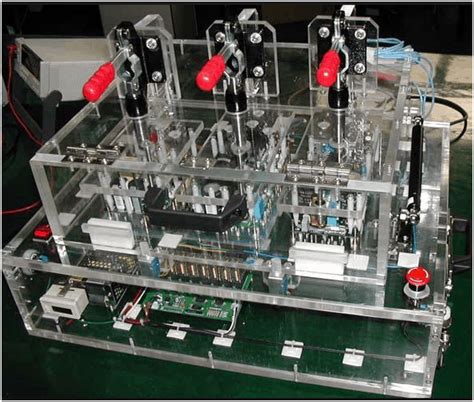
Effective PCB assembly relies on precision engineering to ensure high-efficiency circuit board manufacturing. By integrating automated processes, manufacturers achieve consistent accuracy in component placement, soldering, and testing, which directly impacts electronic performance and reliability. Modern PCBA workflows leverage advanced equipment like pick-and-place machines and automated optical inspection (AOI) systems to minimize human error and accelerate production cycles.
Tip: Prioritize design for manufacturability (DFM) checks early in the PCB assembly process to avoid costly revisions and delays.
Rigorous quality control protocols, including in-circuit testing (ICT) and functional testing, are critical for identifying defects in PCBA units. These steps ensure compliance with industry standards while enhancing product longevity. Additionally, optimizing material selection—such as high-grade substrates and lead-free solder—supports both performance and sustainability goals.
Transitioning to high-efficiency strategies, such as panelization and just-in-time inventory management, reduces waste and lowers production costs. By aligning PCB assembly techniques with evolving technological demands, manufacturers can deliver reliable, high-performance solutions tailored to industries like aerospace, medical devices, and IoT.
Precision PCB Assembly Techniques Explained
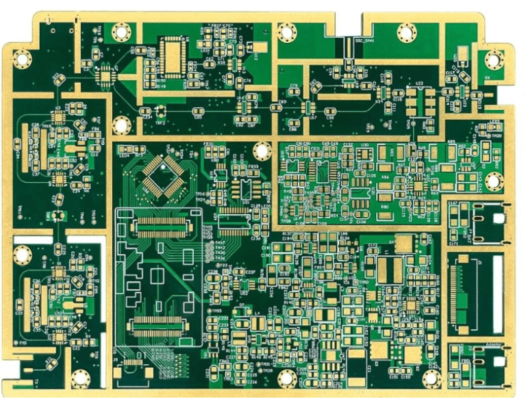
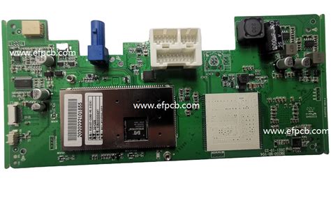
Modern PCB assembly relies on precision engineering to ensure microscopic accuracy in component placement and soldering. Central to this process is PCBA (printed circuit board assembly), which integrates automated systems to minimize human error and enhance repeatability. Techniques such as surface-mount technology (SMT) and through-hole technology (THT) are optimized for specific applications, balancing speed and reliability. For instance, SMT excels in high-density designs, while THT provides robust mechanical bonds for heavier components.
A critical step in PCB assembly is solder paste application, where stencil printing ensures uniform deposition. Advanced pick-and-place machines then position components with tolerances as tight as ±0.025mm. Post-placement, reflow ovens use precise thermal profiles to melt solder without damaging sensitive parts.
| Technique | Key Features | Applications |
|---|---|---|
| SMT | High-speed placement, miniaturization | Consumer electronics, IoT |
| THT | Mechanical durability | Industrial equipment |
Quality assurance in PCBA involves automated optical inspection (AOI) and X-ray testing to detect defects like tombstoning or cold joints. These methods, combined with statistical process control (SPC), ensure consistent output. By integrating these precision techniques, manufacturers achieve high-yield production while meeting stringent performance standards for aerospace, medical devices, and telecommunications.
Automated Circuit Board Manufacturing Processes
Modern PCB assembly relies heavily on automated systems to achieve the precision and scalability required for high-volume production. PCBA (Printed Circuit Board Assembly) workflows now integrate robotic pick-and-place machines, which position components with micron-level accuracy, reducing human error and accelerating throughput. These systems leverage machine vision to verify component orientation and placement, ensuring alignment with design specifications.
Automated soldering techniques, such as reflow ovens and selective soldering systems, further enhance consistency by applying precise temperature profiles to solder joints. This minimizes thermal stress on sensitive components while maintaining electrical reliability. For complex multilayer boards, automated optical inspection (AOI) systems scan for defects like solder bridges or misaligned parts, enabling real-time corrections before final testing.
The adoption of Industry 4.0 principles has transformed PCB assembly lines into interconnected ecosystems. Sensors monitor equipment performance, while data analytics predict maintenance needs, reducing downtime. Automated material handling systems streamline logistics, ensuring components are delivered to assembly stations just-in-time, which cuts waste and optimizes inventory costs.
By integrating PCBA automation, manufacturers achieve faster cycle times, higher yields, and improved repeatability—critical for industries demanding mission-critical reliability, such as aerospace or medical devices. This shift toward smart manufacturing not only elevates quality but also positions firms to adapt swiftly to evolving design requirements and market demands.
Optimizing Electronic Performance With PCB Engineering
Modern PCB assembly relies on precision engineering to enhance electronic performance, balancing signal integrity, thermal management, and component density. By leveraging advanced design software, engineers optimize trace routing and layer stackups to minimize electromagnetic interference (EMI) and power loss. For PCBA (Printed Circuit Board Assembly), material selection plays a critical role—high-frequency laminates and low-loss substrates ensure stable operation in demanding environments like automotive or aerospace systems.
Automated placement systems further refine performance by ensuring micron-level accuracy for components such as ball grid arrays (BGAs) and microcontrollers. This precision reduces parasitic capacitance and inductance, directly improving circuit efficiency. Additionally, thermal simulations guide the strategic placement of heatsinks or vias, preventing hotspots that degrade reliability. Rigorous testing protocols, including in-circuit testing (ICT) and automated optical inspection (AOI), validate electrical continuity and solder joint quality, ensuring every PCB assembly meets performance benchmarks.
By integrating these techniques, manufacturers achieve first-pass yield improvements, reducing rework and accelerating time-to-market. The synergy between design innovation and manufacturing execution underscores how optimized PCBA processes deliver devices capable of sustaining high-speed data transfer, energy efficiency, and long-term durability.
Quality Control in Modern PCB Assembly Lines
Modern PCB assembly lines integrate multilayered quality assurance protocols to ensure zero-defect outcomes in PCBA production. Automated optical inspection (AOI) systems scan boards at micron-level precision, flagging soldering anomalies like bridging or insufficient paste deposition. X-ray imaging complements this by verifying hidden connections in ball grid array (BGA) components, a critical step for high-density designs. In-circuit testing (ICT) and functional testing then validate electrical performance, simulating real-world operating conditions to detect latent failures.
To maintain consistency, statistical process control (SPC) tools analyze production data in real time, identifying trends that could compromise PCB assembly reliability—such as temperature fluctuations in reflow ovens. Environmental stress screening (ESS) further exposes boards to extreme temperatures and vibrations, weeding out units prone to early-life failures. Material traceability systems, powered by barcode or RFID tagging, ensure every component aligns with authenticity certifications, mitigating risks from counterfeit parts.
By harmonizing these strategies, manufacturers achieve first-pass yield rates exceeding 99%, reducing rework costs and accelerating time-to-market for mission-critical applications. This systematic approach not only elevates PCBA durability but also reinforces compliance with industry standards like IPC-A-610 and ISO 9001.
High-Efficiency Circuit Board Production Strategies
Achieving high-efficiency circuit board production requires a strategic blend of process optimization, advanced technologies, and workforce expertise. Central to this approach is the integration of automated PCB assembly systems, which minimize human error while accelerating throughput. By leveraging design for manufacturability (DFM) principles, engineers can preemptively address potential bottlenecks, ensuring smoother transitions from prototyping to full-scale PCBA production.
Key strategies include adopting just-in-time (JIT) inventory management to reduce material waste and implementing modular production lines for flexible scalability. Advanced PCB assembly workflows now incorporate real-time monitoring systems, enabling rapid adjustments to parameters like solder paste application and component placement accuracy. These systems not only enhance yield rates but also align with rigorous quality control protocols, ensuring consistency across high-volume batches.
Furthermore, optimizing thermal management during PCBA processes—such as reflow soldering—prevents component stress, directly contributing to long-term reliability. Collaborative robotics, paired with AI-driven analytics, further refines cycle times and resource allocation. By balancing automation with skilled technician oversight, manufacturers achieve cost-effective yet precision-driven outcomes, meeting the escalating demand for high-efficiency circuit board solutions in industries ranging from consumer electronics to aerospace.
Advanced PCB Assembly Equipment Innovations
Modern PCB assembly workflows are being revolutionized by cutting-edge equipment that bridges the gap between design complexity and manufacturing precision. At the core of this transformation are automated optical inspection (AOI) systems, which employ high-resolution cameras and machine vision algorithms to detect micron-level defects in PCBA components. These systems reduce human error by over 40%, ensuring consistent adherence to IPC-A-610 standards. Equally critical are 3D solder paste inspection (SPI) tools, which map solder deposition accuracy to within ±5μm, preventing downstream reflow issues and minimizing waste.
The integration of robotic pick-and-place machines has redefined scalability in PCB assembly, enabling placement speeds exceeding 25,000 components per hour while handling ultra-miniaturized 01005 packages. Advanced machines now incorporate real-time thermal profiling, dynamically adjusting reflow oven zones to maintain optimal temperature curves for lead-free solder alloys. This capability is vital for preventing tombstoning or voiding in high-density interconnect (HDI) boards.
Emerging technologies like laser direct imaging (LDI) are eliminating photomasks in prototyping, accelerating time-to-market by 30% for complex multilayer designs. Meanwhile, AI-driven predictive maintenance platforms analyze equipment performance data to preemptively address calibration drifts in PCBA lines, reducing unplanned downtime by 22%. These innovations collectively address the dual demands of precision and throughput, particularly for applications requiring automotive-grade reliability or medical-device traceability. By aligning equipment capabilities with evolving PCB assembly requirements, manufacturers achieve defect rates below 50ppm while supporting advanced packaging techniques like embedded components and flexible hybrid electronics.
Streamlining PCB Manufacturing for Reliability
Achieving consistent reliability in PCB assembly requires meticulous attention to both design and production workflows. By integrating automated optical inspection (AOI) and X-ray testing at critical stages, manufacturers can identify latent defects—such as micro-cracks or soldering inconsistencies—before they compromise end-product performance. Modern PCBA lines leverage real-time data analytics to monitor process variables like solder paste viscosity and reflow oven temperature, ensuring adherence to stringent tolerances.
A key strategy involves optimizing design-for-manufacturability (DFM) principles, which reduce complexity while enhancing structural integrity. For instance, implementing standardized pad geometries and balanced copper distribution minimizes thermal stress during operation. Additionally, advanced surface-mount technology (SMT) equipment enables precise component placement at speeds exceeding 25,000 placements per hour, significantly lowering human error risks.
To further bolster reliability, manufacturers are adopting failure mode and effects analysis (FMEA) frameworks during prototyping. This proactive approach identifies potential weak points in PCB assembly layouts, allowing engineers to refine trace routing and grounding schemes before mass production. Combined with rigorous in-circuit testing (ICT) and functional testing (FCT) protocols, these measures create a closed-loop quality system that ensures every PCBA meets or exceeds industry longevity standards.
Cost-Effective PCB Assembly Best Practices
Achieving cost efficiency in PCB assembly requires a strategic balance between quality and budget constraints. One foundational approach involves optimizing material selection without compromising performance. For instance, choosing standardized components over custom parts reduces procurement costs while maintaining compatibility with automated assembly lines. Leveraging PCBA (Printed Circuit Board Assembly) design software to simulate layouts and identify potential manufacturing bottlenecks early can prevent costly rework.
Another critical element is implementing Design for Manufacturability (DFM) principles. By collaborating with engineers to simplify board geometries and minimize layer counts, manufacturers can reduce material waste and streamline production cycles. Automated solder paste application and pick-and-place systems further enhance efficiency, lowering labor costs and human error rates.
Bulk purchasing of common components and negotiating long-term supplier contracts also contribute to cost savings. However, this must align with rigorous inventory management to avoid obsolescence risks. Additionally, adopting modular PCB assembly processes allows manufacturers to reuse proven subassemblies across multiple projects, cutting development time and expenses.
Finally, integrating statistical process control (SPC) tools ensures consistent quality while identifying inefficiencies in real time. Pairing this with selective testing—such as in-circuit testing (ICT) for critical nodes instead of full-board diagnostics—optimizes resource allocation. By prioritizing these strategies, companies can deliver high-reliability PCBA solutions at competitive prices, aligning with broader industry demands for scalable, economical electronics manufacturing.
Conclusion
The evolution of PCB assembly (PCBA) underscores the critical balance between precision engineering and scalable manufacturing practices. By integrating automated processes with rigorous quality assurance protocols, manufacturers ensure that high-efficiency circuit boards meet the exacting demands of modern electronics. Innovations in surface-mount technology and automated optical inspection (AOI) systems have streamlined production timelines while minimizing human error, directly enhancing end-product reliability.
Adopting cost-effective strategies, such as panelized assembly and optimized component placement, further elevates yield rates without compromising performance. As the industry shifts toward IoT and miniaturized devices, the role of advanced PCBA workflows becomes indispensable in maintaining signal integrity and thermal management. By prioritizing data-driven process refinement and investing in next-generation equipment, manufacturers can sustainably address both current and emerging challenges. Ultimately, the convergence of precision PCB assembly techniques with adaptive manufacturing frameworks solidifies the foundation for innovation across industries reliant on robust electronic systems.
Frequently Asked Questions
What distinguishes PCB assembly from PCBA?
PCB assembly refers to the process of populating a bare circuit board with electronic components, while PCBA (Printed Circuit Board Assembly) denotes the completed, functional board ready for integration into devices. Both terms emphasize different stages of the same manufacturing workflow.
How does thermal management impact PCB reliability?
Effective thermal management ensures components operate within safe temperature ranges, preventing overheating and prolonging lifespan. Techniques like copper pours and heat sinks are critical in high-power PCBA designs to maintain performance stability.
What quality checks are essential in modern PCB assembly?
Automated optical inspection (AOI), X-ray testing, and functional testing validate solder joint integrity, component alignment, and electrical performance. These steps align with rigorous quality control protocols to minimize defects.
Can automated assembly reduce production costs?
Yes, automated pick-and-place systems and reflow soldering streamline workflows, cutting labor costs and human error. This efficiency enables scalable, high-volume production without compromising PCBA precision.
How do designers optimize PCB layouts for manufacturability?
Adhering to design for manufacturability (DFM) guidelines—such as standardized component spacing and panelization—ensures compatibility with automated assembly equipment, reducing rework and accelerating time-to-market.
Ready to Elevate Your PCB Assembly Workflow?
For tailored solutions in high-efficiency circuit board manufacturing, please click here to explore advanced PCBA services tailored to your project’s needs.