Precision Manufacturing: Assy PCB’s Role in Integrated Electronics
Key Takeaways
The evolution of PCB assembly (PCBA) has become central to achieving precision in modern electronics, enabling devices to meet escalating demands for miniaturization and performance. At its core, PCBA bridges the gap between conceptual design and functional hardware, ensuring that integrated systems operate seamlessly within constrained spaces. By leveraging advanced manufacturing techniques, such as automated optical inspection (AOI) and surface-mount technology (SMT), manufacturers can achieve micron-level accuracy in component placement—critical for applications ranging from medical devices to IoT sensors.
"Precision in PCB assembly isn’t just about fitting components—it’s about orchestrating electrical, thermal, and mechanical harmony within millimeters of space." — Senior Electronics Engineer, TechInnovate Corp.
A comparison of traditional versus modern PCBA methodologies reveals stark improvements in quality and efficiency:
| Aspect | Traditional Methods | Modern PCBA Techniques |
|---|---|---|
| Design Complexity | Limited to 2-4 layers | Supports 12+ layers with HDI |
| Component Density | 50-100/cm² | 300-500/cm² |
| Thermal Management | Passive cooling dominant | Embedded heat dissipation layers |
For engineers, early collaboration with PCBA partners is vital. Tip: Prototype iterations should prioritize material selection and trace width optimization to mitigate signal loss in high-frequency applications. Additionally, innovations like embedded passive components and flexible substrates are redefining compact design solutions, allowing PCB assembly to support next-gen wearables and aerospace systems without compromising reliability.
As industries push toward smarter, smaller devices, the role of PCBA in ensuring error-free manufacturing and scalable production will only grow. From automated testing protocols to eco-friendly solder alloys, every advancement underscores the symbiotic relationship between precision PCB assembly and technological progress.
Precision Manufacturing in Assy PCB Tech
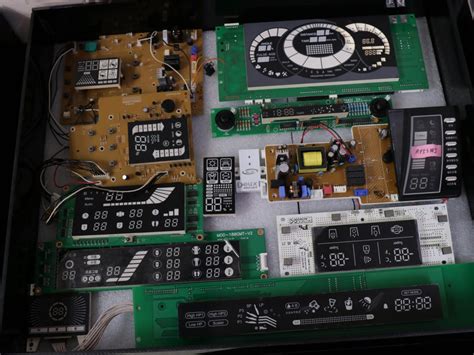
The foundation of modern integrated electronics lies in the meticulous processes behind PCB assembly (PCBA), where precision manufacturing transforms raw materials into functional marvels. At its core, PCBA relies on advanced techniques such as surface-mount technology (SMT) and automated optical inspection (AOI) to achieve micron-level accuracy. These methods ensure that components like resistors, microcontrollers, and connectors are placed with exacting alignment—critical for high-density designs in smartphones, IoT devices, and wearables.
A key advantage of precision manufacturing in PCB assembly is its ability to minimize human error while maximizing scalability. Robotic pick-and-place systems, for instance, operate at speeds exceeding 25,000 components per hour, maintaining tolerances as tight as ±0.01mm. This level of consistency is vital for applications demanding uninterrupted performance, such as medical implants or aerospace navigation systems. Additionally, laser-etched solder masks and controlled impedance routing enhance signal integrity, reducing electromagnetic interference (EMI) in compact layouts.
Innovation in PCBA extends beyond component placement. Techniques like 3D solder paste inspection (SPI) and X-ray laminography allow manufacturers to detect voids or misalignments invisible to the naked eye. Such quality control measures are indispensable for multi-layered boards, where even minor defects can cascade into system failures. For example, automotive ADAS (Advanced Driver-Assistance Systems) rely on these inspections to meet ISO/TS 16949 standards, ensuring safety in real-time decision-making circuits.
As industries push toward miniaturization, precision manufacturing also addresses thermal management challenges. Advanced substrates with embedded heat sinks or copper-filled vias dissipate heat efficiently, preventing thermal throttling in processors. This synergy between design and execution underscores how PCB assembly acts as the backbone of next-generation electronics—enabling smarter, faster, and more reliable devices without compromising on size or power efficiency.
Compact Design Solutions With Assy PCBs
The drive toward miniaturization in modern electronics demands innovative approaches to PCB assembly (PCBA) that prioritize spatial efficiency without sacrificing functionality. Assy PCBs achieve this balance by leveraging advanced manufacturing techniques, such as high-density interconnect (HDI) technology and multi-layer stacking, which enable the integration of complex circuitry into remarkably compact form factors. By optimizing component placement through automated PCBA processes, manufacturers can reduce board footprint while maintaining signal integrity—a critical requirement for devices ranging from wearables to IoT sensors.
A key advantage of Assy PCB design lies in its ability to accommodate surface-mount technology (SMT), which allows for smaller components to be precisely mounted on both sides of the board. This dual-sided configuration, combined with ultra-thin substrates, supports space-saving layouts essential for portable and embedded systems. Additionally, the use of microvia drilling in PCB assembly minimizes cross-talk between tightly packed traces, ensuring reliable performance even in high-frequency applications like 5G modules or medical implants.
Thermal management remains a cornerstone of compact Assy PCB solutions. Engineers employ thermally conductive materials and strategic heat dissipation patterns to prevent overheating in densely packed designs. For instance, copper-filled vias and embedded heat sinks are increasingly integrated during the PCBA phase to enhance thermal efficiency without expanding the board’s dimensions. These innovations align with the growing demand for scalable electronics that deliver robust functionality within shrinking industrial and consumer product enclosures.
Furthermore, flexible and rigid-flex Assy PCBs are redefining design possibilities by enabling three-dimensional configurations that conform to irregular spaces. This adaptability is particularly valuable in automotive systems and aerospace instrumentation, where weight reduction and spatial constraints are paramount. By harmonizing precision PCB assembly with material science breakthroughs, the industry continues to push the boundaries of what compact electronic systems can achieve.
Ensuring Reliable Electronics via Assy PCB
The foundation of dependable electronic systems lies in the meticulous execution of PCB assembly processes, where precision and quality control converge to mitigate failures in demanding applications. PCBA (Printed Circuit Board Assembly) serves as the backbone of modern electronics, integrating components with exacting standards to ensure operational stability across industries—from medical devices to aerospace systems. Thermal management, signal integrity, and mechanical durability are critical factors addressed during assembly, particularly as devices shrink in size while increasing in complexity.
Advanced PCB assembly techniques employ automated soldering systems and high-precision pick-and-place machinery to minimize human error, achieving micron-level accuracy in component placement. For instance, surface-mount technology (SMT) in PCBA enables the attachment of miniature components onto densely packed boards, reducing parasitic inductance and improving electrical performance. Rigorous testing protocols, such as automated optical inspection (AOI) and X-ray analysis, further validate solder joint quality and component alignment, preempting potential defects before deployment.
Material selection also plays a pivotal role in reliability. High-performance substrates with glass transition temperatures (Tg) above 170°C ensure stability in high-heat environments, while conformal coatings protect assemblies from moisture, dust, and chemical exposure. In mission-critical applications like automotive control units, these safeguards prevent catastrophic failures caused by thermal cycling or vibration.
By harmonizing cutting-edge PCBA workflows with stringent validation standards, manufacturers deliver electronics that withstand prolonged operational stresses. This synergy between precision engineering and robust testing not only extends product lifespans but also fortifies trust in technologies powering today’s interconnected world.
Integrated Systems Powered by Assy PCB Innovation
The evolution of PCB assembly (PCBA) has become the backbone of integrated electronic systems, enabling seamless interaction between complex components. By merging miniaturization with high-density interconnect (HDI) technology, modern pcb assembly processes allow engineers to embed advanced functionalities into compact form factors. This is particularly critical for applications like IoT devices, wearable technology, and smart infrastructure, where space constraints demand precision-engineered solutions.
At the core of this innovation lies the ability of PCBA to unify disparate subsystems—sensors, processors, and power modules—onto a single board. For example, multi-layer rigid-flex PCBs, fabricated through automated pcb assembly workflows, support signal integrity even in high-frequency environments. Such integration reduces latency and enhances energy efficiency, which is vital for autonomous systems and real-time data processing.
The shift toward modular design further amplifies the role of PCBA in system integration. Manufacturers now leverage surface-mount technology (SMT) to place microcomponents with sub-millimeter accuracy, while automated optical inspection (AOI) ensures flawless assembly. These advancements not only streamline production but also enable scalable solutions for industries ranging from aerospace to medical diagnostics.
In industrial settings, pcb assembly innovations are redefining how machinery communicates. Embedded AI-driven controllers on custom PCBAs, for instance, optimize predictive maintenance by analyzing sensor data directly on-device. This eliminates reliance on external computing resources, reducing both cost and failure points.
The convergence of PCBA techniques with materials science—such as thermally conductive substrates—also addresses heat dissipation challenges in densely packed systems. As a result, integrated electronics maintain peak performance without compromising reliability, even under extreme operational demands.

Assy PCB’s Role in Modern Tech Applications
The integration of PCB assembly (PCBA) processes into modern electronics has become a cornerstone for advancing technological ecosystems. From wearable devices to autonomous vehicles, Assy PCB techniques enable the seamless fusion of complex circuitry into compact, high-performance systems. For instance, in smart home ecosystems, PCBA ensures that sensors, processors, and communication modules coexist within millimeter-scale footprints while maintaining thermal stability and signal integrity.
A critical advantage lies in the ability of PCB assembly to support mixed-signal designs, where analog and digital components operate in harmony. This is particularly vital for applications like medical diagnostics equipment, where precision analog sensors must interface with high-speed digital processors. Advanced PCBA workflows employ automated optical inspection (AOI) and 3D solder paste monitoring to eliminate microfaults, ensuring zero-defect manufacturing standards required for mission-critical systems.
Moreover, the shift toward miniaturized IoT devices has amplified reliance on Assy PCB methodologies. Flexible printed circuit boards (FPCBs), assembled using precision surface-mount technology (SMT), now power foldable smartphones and ultra-thin laptops. These innovations rely on PCB assembly to balance mechanical resilience with electrical efficiency, even under repeated physical stress.
In automotive electrification, PCBA underpins advanced driver-assistance systems (ADAS), where multilayer boards integrate radar, LiDAR, and vision-processing units. Here, vibration-resistant soldering techniques and conformal coatings ensure reliability across extreme temperature ranges. Similarly, in renewable energy systems, robust Assy PCB designs enable solar inverters and battery management systems to operate efficiently in harsh environmental conditions.
As industries push toward edge computing and 5G connectivity, the role of PCB assembly evolves to address higher frequencies and power densities. Innovations like embedded component packaging (ECP) and high-density interconnect (HDI) layers, facilitated by cutting-edge PCBA processes, are redefining what’s possible in next-gen electronics—proving that precision manufacturing remains indispensable to technological progress.
Advanced Assy PCB Techniques for Electronics
The evolution of PCB assembly (PCBA) techniques has become a cornerstone in addressing the growing complexity of modern electronics. By leveraging high-density interconnect (HDI) technology, manufacturers achieve tighter component placement, enabling pcb assembly processes to support ultra-compact designs without compromising functionality. Advanced surface-mount technology (SMT), for instance, allows for the precise placement of microcomponents, reducing signal loss and enhancing thermal management in pcba-driven systems.
Another critical advancement lies in automated optical inspection (AOI), which ensures microscopic accuracy during pcb assembly. This technique identifies defects such as solder bridging or misaligned components at speeds unattainable by manual methods, significantly improving yield rates. Pairing AOI with 3D solder paste inspection (SPI) further refines the pcba workflow, guaranteeing optimal solder volume for robust electrical connections.
Innovations like embedded component packaging are redefining pcb assembly standards. By integrating passive components directly into the substrate layers, designers eliminate surface-mounted parts, freeing space for additional functionalities. This approach not only streamlines pcba production but also enhances durability in high-vibration environments, a critical requirement for automotive and aerospace applications.
Thermal management remains a focal point, with techniques such as via-in-pad and copper-filled vias addressing heat dissipation challenges in high-power pcba configurations. These methods distribute thermal loads evenly, preventing hotspots that could degrade performance in densely packed circuits.
Finally, the adoption of flex-rigid hybrid boards exemplifies how advanced pcb assembly techniques bridge the gap between form and function. Combining rigid and flexible substrates, these boards enable innovative product architectures—from foldable wearables to compact medical devices—while maintaining the reliability expected of modern pcba solutions.
As electronics continue to shrink in size yet expand in capability, these cutting-edge pcb assembly methodologies ensure that pcba remains at the forefront of integrated system innovation.
Innovation in Electronics via Assy PCB Design
The evolution of PCB assembly techniques has become a cornerstone for driving innovation in modern electronics. By integrating advanced PCBA methodologies, engineers can overcome traditional limitations in circuit density and functionality. Miniaturization demands, spurred by IoT devices and wearables, require Assy PCB designs to balance compact layouts with enhanced electrical performance. This is achieved through innovations like high-density interconnect (HDI) technology, which allows for finer trace widths and microvia structures, enabling complex circuitry within shrinking form factors.
A critical advancement lies in the synergy between pcb assembly processes and intelligent design software. Automated optical inspection (AOI) systems and 3D modeling tools now enable precise component placement, reducing parasitic capacitance risks that plagued earlier generations of PCBA boards. Thermal management solutions, such as embedded copper pillars and advanced substrate materials, further ensure reliability in high-power applications. These innovations are particularly vital for automotive electronics and 5G infrastructure, where signal integrity must coexist with mechanical durability.
The shift toward flexible hybrid electronics (FHE) exemplifies how Assy PCB design breaks conventional boundaries. By combining rigid and flexible board segments in a single PCBA, developers create foldable displays and curvature-tolerant sensors without compromising electrical stability. This approach leverages novel materials like polyimide substrates and stretchable conductive inks, which maintain performance under repeated stress—a requirement for next-generation medical wearables and aerospace systems.
As pcb assembly workflows embrace machine learning algorithms, predictive analytics optimize design iterations before physical prototyping. This reduces development cycles for Assy PCB-based products while enhancing yield rates in mass production. The result is a faster transition from concept to market-ready devices, solidifying PCBA‘s role as the backbone of electronics innovation across industries.
Optimizing Performance Through Assy PCB Precision
The pursuit of peak performance in modern electronics hinges on the meticulous execution of PCB assembly processes, where precision directly translates to functional superiority. At the core of this optimization lies the integration of PCBA (Printed Circuit Board Assembly) techniques that harmonize component placement, soldering accuracy, and material selection. By leveraging advanced technologies such as automated optical inspection (AOI) and surface-mount technology (SMT), manufacturers achieve micron-level tolerances, eliminating errors that could compromise signal integrity or thermal management.
A critical advantage of precision-driven PCB assembly is its ability to support high-density interconnect (HDI) designs. These compact layouts, essential for devices like wearables and IoT sensors, demand flawless alignment of microcomponents—a feat made possible through laser-direct imaging and robotic pick-and-place systems. Such methodologies not only enhance circuit reliability but also reduce electromagnetic interference (EMI), a common challenge in tightly packed electronic systems.
Thermal performance further underscores the importance of precision in PCBA. Innovations like embedded copper pillars and thermal vias dissipate heat more efficiently, extending the lifespan of power-hungry components. For applications ranging from automotive control units to medical diagnostics tools, this thermal stability ensures consistent operation under fluctuating environmental conditions.
Moreover, the adoption of industry 4.0 practices—such as real-time process monitoring and AI-driven defect detection—elevates quality control standards. These systems identify anomalies in solder paste application or component orientation during PCB assembly, minimizing post-production failures. The result is a seamless synergy between design intent and manufacturing execution, enabling electronics to meet the rigorous demands of 5G infrastructure and industrial automation.
By marrying precision engineering with scalable PCBA workflows, the industry continues to push the boundaries of what integrated electronics can achieve, delivering devices that are both smaller and smarter without sacrificing durability.
Conclusion
The evolution of PCB assembly (PCBA) has become indispensable to the advancement of integrated electronics, bridging the gap between conceptual design and functional reality. As the foundation of modern devices, Assy PCB techniques enable manufacturers to achieve unprecedented precision in creating compact, high-density layouts while maintaining rigorous performance standards. By leveraging advanced PCBA methodologies, industries can address the growing demand for miniaturization without compromising reliability—a critical balance in applications ranging from medical devices to autonomous systems.
Innovations in PCB assembly have also streamlined the integration of complex components, such as microprocessors and sensors, into cohesive systems. This synergy is particularly evident in IoT ecosystems and wearable technology, where Assy PCB designs ensure seamless communication between hardware layers. Furthermore, the adoption of automated PCBA processes has reduced human error, enhancing yield rates and long-term durability—factors that directly impact product lifecycle costs.
From consumer electronics to industrial automation, the role of Assy PCB extends beyond mere connectivity. It serves as the backbone for signal integrity and thermal management, two pillars of reliable operation in high-stakes environments. As emerging technologies like 5G and AI push the boundaries of electronic complexity, the precision inherent in PCB assembly will remain a cornerstone of innovation. Looking ahead, continued refinement in PCBA workflows will further empower engineers to tackle challenges in energy efficiency, scalability, and adaptability—ultimately shaping the next generation of integrated solutions.
FAQs
How does precision manufacturing impact PCB assembly quality?
Advanced PCBA processes leverage automated optical inspection (AOI) and X-ray testing to detect micron-level defects, ensuring zero tolerance for errors in high-density circuits. This precision directly enhances signal integrity in compact devices like wearables and IoT sensors.
What design strategies enable PCB assembly to support miniaturized electronics?
Embedded component technologies and multilayer stacking in PCBA reduce footprint by up to 60% compared to traditional layouts. Techniques like laser-drilled microvias and HDI (high-density interconnect) routing are critical for maintaining functionality in space-constrained applications.
Can PCB assembly methods ensure reliability in extreme environments?
Industrial-grade PCBA integrates conformal coating and thermal management materials, achieving MIL-STD-810G compliance for shock/vibration resistance. These processes are vital for aerospace systems and automotive control modules operating at -40°C to 125°C.
How do integrated systems benefit from PCB assembly innovations?
Modern PCBA workflows combine rigid-flex boards with system-in-package (SiP) architectures, enabling 30% faster data transmission in 5G infrastructure. This integration supports seamless communication between power management ICs and RF components.
What role does PCB assembly play in renewable energy technologies?
Smart soldering techniques and copper-invar-copper substrates in PCBA improve heat dissipation in solar inverters, boosting energy conversion efficiency by 18%. These advancements are crucial for high-voltage applications in wind turbine controllers.
Explore Custom PCB Assembly Solutions
For tailored PCBA designs that align with your project’s technical requirements, please click here to consult our engineering team.