Precision Methods for Compact PCB Assembly and Component Testing
Key Takeaways
Effective PCB assembly and testing in compact designs demand specialized approaches to address space constraints and ensure reliability. PCBA (Printed Circuit Board Assembly) processes for miniaturized electronics require precision soldering techniques, such as micro-soldering with temperature-controlled irons or laser-assisted systems, to avoid damaging sensitive components. Automated optical inspection (AOI) systems are critical for detecting microscopic defects like solder bridges or misalignments, which are common in densely packed layouts.
Tip: When working with high-density boards, prioritize thermal management during component placement to prevent localized overheating during operation.
Functional verification often involves boundary scan testing or in-circuit testing (ICT) to validate electrical performance without physical probes. Challenges such as signal interference in tight spaces can be mitigated through strategic shielding and optimized trace routing. For PCB assembly success, adhere to IPC-A-610 standards for solder joint quality, and leverage 3D X-ray inspection for hidden connections in multi-layer designs. Combining these methods ensures robust PCBA outcomes, balancing miniaturization with durability in modern electronics.
Precision Soldering for Compact PCBs
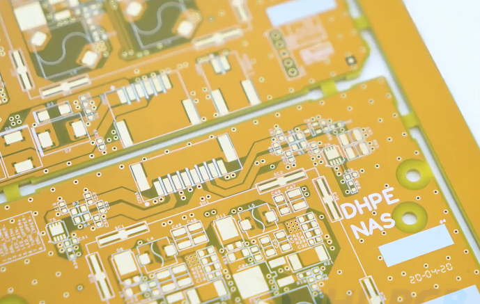
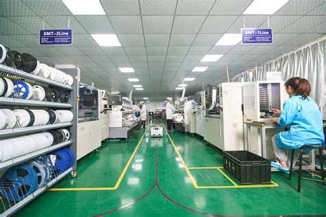
Achieving reliable PCB assembly in compact designs demands meticulous attention to soldering techniques. Miniaturized components, such as 0402 or 0201 packages, require precision tools like micro-tip soldering irons and magnified inspection systems. Thermal management becomes critical, as excessive heat can damage adjacent components or warp delicate substrates. For PCBA (Printed Circuit Board Assembly) involving high-density interconnects, reflow soldering with tightly controlled temperature profiles ensures consistent joint formation while minimizing voids.
| Technique | Application | Key Benefit |
|---|---|---|
| Hand Soldering | Prototyping, rework | Flexibility for small batches |
| Reflow Soldering | Surface-mount components | High repeatability for mass production |
| Selective Soldering | Mixed-technology boards | Precision for heat-sensitive parts |
Automated optical inspection (AOI) systems often complement these processes, identifying defects like bridging or cold joints early in the PCB assembly workflow. For ultra-fine-pitch components, solder paste stencils with apertures below 100µm ensure accurate deposition. Engineers must also consider solder alloy selection—lead-free SAC305, for instance, balances reliability with environmental compliance. By integrating these methods, PCBA teams can maintain electrical integrity while navigating the spatial constraints of modern compact designs, paving the way for subsequent functional verification stages.

Automated Inspection in PCB Assembly
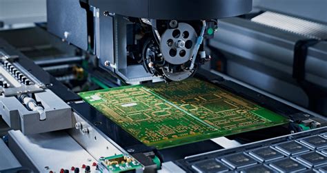
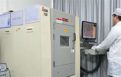
Modern PCB assembly processes demand rigorous quality control, particularly in compact designs where component density creates unique challenges. Automated optical inspection (AOI) systems have become indispensable in PCBA workflows, utilizing high-resolution cameras and machine learning algorithms to detect microscopic defects like solder bridging or misaligned components. These systems achieve sub-micron accuracy, scanning hundreds of connections per minute – a task impractical for manual inspection. For hidden joints, automated X-ray inspection (AXI) complements AOI by penetrating multilayer boards to verify BGA (ball grid array) soldering integrity.
Integration with design-for-test (DFT) principles ensures inspection systems align with layout constraints, minimizing false positives in tight spaces. Advanced PCBA lines now combine inline AOI with real-time process feedback, enabling immediate corrections during reflow or placement stages. This closed-loop approach reduces rework cycles by up to 40% in miniaturized electronics. However, balancing inspection speed and resolution remains critical, as excessive throughput can compromise defect detection in ultra-fine-pitch components.
Transitioning to functional verification, these automated methods establish a foundation for reliability by eliminating assembly-related faults early, ensuring subsequent tests focus on performance validation rather than correcting manufacturing errors.
Functional Testing of Miniature Electronics
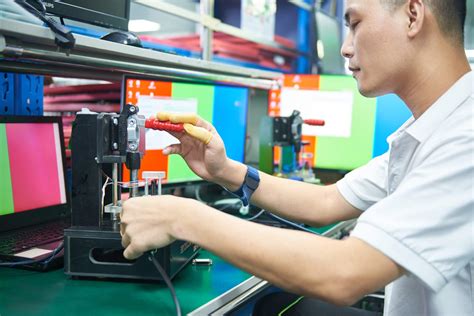
Functional testing forms the critical final stage in PCB assembly workflows, ensuring that miniaturized electronics operate as intended under real-world conditions. For PCBA (printed circuit board assembly) designs with dense layouts, engineers employ boundary scan testing and JTAG protocols to validate signal integrity across tightly packed components. Automated test equipment (ATE) simulates operational scenarios, verifying voltage regulation, communication protocols, and power consumption metrics while identifying latent defects like solder bridges or micro-cracks.
In compact designs, thermal stress testing becomes indispensable, as heat dissipation challenges escalate with reduced board space. Environmental chambers subject assemblies to temperature cycling, exposing weaknesses in component adhesion or material fatigue. Additionally, automated optical inspection (AOI) systems complement functional tests by cross-referencing electrical performance with visual anomalies missed during earlier PCB assembly stages. For high-frequency applications, vector network analyzers measure impedance mismatches, ensuring signal fidelity in miniature RF circuits.
Transitioning from validation to scalability, test protocols must balance rigor with efficiency—especially for high-volume PCBA production. Modular test jigs and reconfigurable software frameworks enable rapid adaptation across product variants, minimizing downtime. By integrating these strategies, manufacturers mitigate risks of field failures while aligning with evolving demands for smaller, yet more reliable, electronic systems.
Challenges in Miniature PCB Component Testing
Testing electronic components on compact PCBA introduces unique obstacles due to shrinking board sizes and higher component density. A primary challenge lies in achieving reliable electrical contact during PCB assembly, as miniature solder joints and tightly packed traces leave minimal room for traditional probe-based testing. Thermal management becomes critical when validating high-power components in confined spaces, where localized heat buildup can skew test results or damage adjacent parts. Additionally, automated optical inspection (AOI) systems face limitations in detecting micro-scale defects, such as hairline cracks or insufficient solder on ultra-small pads, necessitating advanced imaging techniques or X-ray inspection.
Signal integrity verification adds complexity, as crosstalk and electromagnetic interference (EMI) are amplified in densely populated layouts. Engineers must balance test coverage with physical constraints, often requiring custom jigs or reconfigurable test platforms tailored to specific PCBA designs. The interdependence of component placement and testability further complicates functional validation, demanding close collaboration between design and manufacturing teams. While innovations like boundary-scan testing mitigate some accessibility issues, the evolving demand for miniaturization ensures these challenges remain at the forefront of compact electronics development.
Ensuring Reliability in Compact PCB Designs
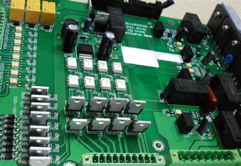
Achieving long-term reliability in PCB assembly for compact designs requires meticulous attention to both material selection and manufacturing processes. As PCBA (Printed Circuit Board Assembly) scales down, factors like thermal stress, signal interference, and mechanical stability become critical. Designers must prioritize high-density interconnects that minimize parasitic capacitance while maintaining robust electrical pathways. Techniques such as via-in-pad and microvia stacking enhance space utilization without compromising structural integrity.
Thermal management is equally vital, particularly when integrating power-dense components. Using thermally conductive substrates and strategic copper balancing helps dissipate heat efficiently, preventing premature failure. For validation, automated optical inspection (AOI) and X-ray imaging are indispensable for detecting micro-solder joint defects or misalignments invisible to the naked eye.
Functional testing under simulated operational conditions—such as temperature cycling and vibration tests—ensures that miniaturized electronics withstand real-world demands. Additionally, adherence to IPC-A-610 standards for PCB assembly guarantees consistent quality across batches. By combining advanced design practices with rigorous testing protocols, engineers can mitigate risks inherent to PCBA in compact form factors, ensuring both performance and durability.
Optimizing Component Placement for Small PCBs
Effective PCB assembly of miniaturized electronics demands meticulous planning of component placement to balance spatial constraints with performance requirements. In PCBA workflows, designers must prioritize signal integrity and thermal management while accommodating high-density layouts. Start by grouping components based on functional blocks and power requirements, ensuring high-speed traces are minimized to reduce electromagnetic interference. Symmetrical arrangements for paired circuits, such as differential signals, can further enhance stability in compact designs.
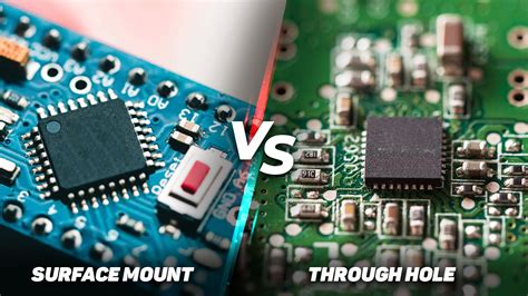
Automated placement tools integrated into PCB assembly software enable precise alignment of surface-mount devices (SMDs), particularly for components like 0402 or 0201 packages. However, manual adjustments are often necessary to avoid mechanical conflicts with connectors or heat sinks. Critical considerations include maintaining adequate clearance for rework tools and aligning test points for accessibility during PCBA validation phases.
Thermal hotspots can be mitigated by positioning heat-generating components away from sensitive analog circuits, leveraging thermal vias or copper pours for dissipation. Additionally, adherence to design-for-manufacturing (DFM) guidelines ensures compatibility with pick-and-place machines and reflow profiles, minimizing defects in high-volume production. By harmonizing electrical, thermal, and mechanical factors, engineers achieve reliable PCB assembly outcomes even in space-constrained applications.
Advanced Techniques for PCB Functional Verification
Functional verification is a critical phase in PCB assembly, ensuring that miniaturized electronics operate as intended under real-world conditions. For compact PCBA designs, engineers increasingly rely on automated test equipment (ATE) to validate signal integrity, power distribution, and communication protocols. Boundary scan testing, for instance, enables non-invasive inspection of densely packed components by leveraging IEEE 1149.1 standards to isolate faults in interconnected circuits.
Another advanced method involves in-circuit testing (ICT), which verifies the electrical performance of individual components after PCB assembly. This technique is particularly effective for identifying soldering defects or mismatched tolerances in high-density layouts. To address thermal challenges in miniaturized systems, thermal cycling tests simulate extreme operating temperatures, exposing weaknesses in solder joints or material stability.
For PCBA designs with embedded firmware, functional verification often integrates software-driven diagnostics. Tools like script-based test suites validate firmware interactions with hardware, ensuring seamless operation of microcontrollers or sensors. Additionally, automated optical inspection (AOI) systems, though primarily used during assembly, can be repurposed to cross-check component alignment and orientation post-soldering.
Transitioning from validation to reliability assurance, these techniques bridge gaps between design intent and operational reality. By combining data-driven analysis with iterative testing protocols, manufacturers mitigate risks in compact electronics, aligning with the broader goals of precision and durability outlined in earlier sections.
Best Practices for Miniaturized Electronics Testing
Effective testing of miniaturized electronics demands meticulous attention to detail, particularly in PCB assembly and PCBA workflows. Thermal management and signal integrity testing are critical steps, given the limited space for heat dissipation and the proximity of high-density components. Automated tools like automated optical inspection (AOI) and X-ray inspection help identify soldering defects, such as micro-cracks or insufficient solder joints, which are common in compact designs.
For functional verification, engineers should prioritize boundary scan testing to validate interconnects without physical probes, reducing the risk of damaging delicate traces. Additionally, in-circuit testing (ICT) ensures each component operates within specified parameters, even in tightly packed layouts. To maintain consistency, implement environmental stress screening (ESS), exposing assemblies to temperature cycles and vibration to simulate real-world conditions.
A key challenge lies in balancing test coverage with efficiency. Leveraging design-for-testability (DFT) principles during the PCB assembly phase—such as adding test points or modularizing circuits—streamlines diagnostics. Finally, document all test protocols rigorously, ensuring traceability for post-production analysis. By integrating these practices, manufacturers can achieve reliable PCBA outcomes while addressing the unique demands of miniaturized electronics.
Conclusion
The evolution of PCB assembly processes for compact designs underscores the importance of integrating precision techniques with rigorous validation protocols. As miniaturized electronics push the boundaries of component density, automated optical inspection (AOI) and X-ray testing have become indispensable in PCBA workflows, ensuring solder joint integrity and alignment accuracy. However, achieving reliability extends beyond assembly—functional verification through boundary-scan testing and environmental stress screening (ESS) remains critical to address latent defects in high-density layouts.
To sustain performance in constrained spaces, engineers must balance advanced PCB assembly methods with proactive design-for-test (DFT) strategies. This includes optimizing test-point accessibility and leveraging in-circuit testing (ICT) for real-time diagnostics. While challenges like thermal management persist, adopting standardized protocols across PCBA stages—from solder paste application to final validation—ensures consistent outcomes. Ultimately, the synergy between precision manufacturing and comprehensive testing defines success in an era where compactness and reliability are non-negotiable.
Frequently Asked Questions
What distinguishes PCB assembly from PCBA in compact electronics?
PCB assembly refers to the process of mounting components onto a bare circuit board, while PCBA (Printed Circuit Board Assembly) includes both assembly and subsequent testing phases. For miniaturized designs, precise PCB assembly ensures components fit within tight spaces, and PCBA validates functionality through automated inspection and electrical testing.
How does automated inspection improve quality in miniature PCB assembly?
Automated Optical Inspection (AOI) and X-ray systems detect solder defects, misalignments, and micro-scale flaws invisible to the human eye. These tools are critical for high-density interconnects in compact designs, reducing failure rates by over 70% in PCBA workflows.
What challenges arise during functional testing of miniaturized electronics?
Limited physical access to test points and signal interference from densely packed components complicate testing. Solutions include using bed-of-nails fixtures for parallel testing and implementing boundary-scan techniques to isolate individual circuit paths.
Why is thermal management crucial in compact PCB designs?
Miniature layouts concentrate heat-generating components, risking thermal stress. Techniques like thermal vias and strategic placement of passive components mitigate hotspots, ensuring long-term reliability post-PCB assembly.
How can component placement optimize small PCB performance?
Prioritize high-speed traces and sensitive analog circuits away from noise sources. Automated placement algorithms balance spatial constraints with signal integrity requirements, a key step in advanced PCBA processes.
Explore Professional PCB Assembly Solutions
For tailored support in high-precision PCB assembly and PCBA testing, please click here to connect with industry experts.