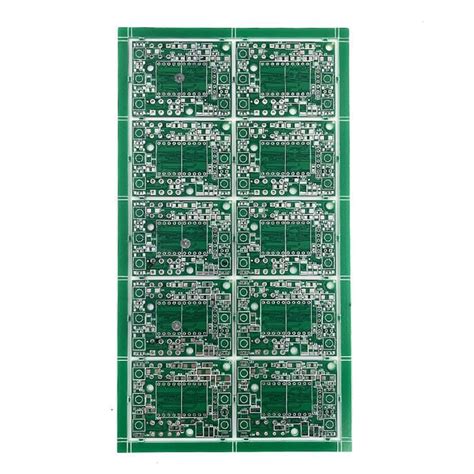
Precision Multilayer PCB Fabrication Techniques
Key Takeaways
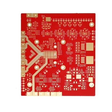
When selecting PCB manufacturing partners, understanding core technical elements ensures optimal performance and cost-efficiency. Multilayer PCB layer stackup optimization directly impacts signal integrity, with 4-30 layer configurations balancing complexity and PCB manufacturing cost. FR-4 material selection remains critical for thermal stability, while surface finishes like Immersion Gold (ENIG) and HASL cater to diverse environmental and solderability needs.
For rigid-flex PCB design strategies, balancing mechanical durability with high-density routing requires collaboration with experienced PCB manufacturing companies. Advanced techniques such as buried copper technology enhance thermal management in power electronics, though they may influence PCB manufacturing business timelines due to added complexity.
| Factor | Consideration |
|---|---|
| Surface Finish | ENIG for fine-pitch components; HASL for cost |
| Layer Count | Higher layers = higher reliability + cost |
| Material Choice | FR-4 for general use; specialized substrates for high-frequency |
Strict quality control testing protocols, including impedance checks and microsection analysis, ensure compliance with industry standards. By aligning design goals with PCB manufacturing capabilities, you mitigate risks and achieve scalable solutions for high-performance electronics.
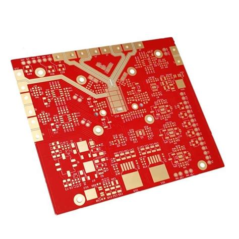
Multilayer PCB Layer Stackup Optimization
When planning multilayer PCB layer stackup optimization, you must balance electrical performance with PCB manufacturing cost considerations. The arrangement of signal, power, and ground layers directly impacts signal integrity, thermal management, and impedance control. For high-density designs, PCB manufacturing companies often recommend symmetrical stackups to minimize warpage while ensuring consistent dielectric spacing between layers.
Proper optimization requires analyzing material properties—like FR-4’s glass transition temperature—and aligning them with operational demands. Thinner prepreg layers reduce cross-talk in high-speed circuits, but tighter tolerances increase PCB manufacturing business expenses. To avoid overspending, prioritize critical layers (e.g., RF or high-voltage sections) and use cost-effective configurations for less sensitive areas.
Advanced tools, such as field solvers, help simulate electromagnetic behavior before production. Pairing these with buried via strategies and copper weight adjustments ensures optimal current distribution without compromising fabrication feasibility. Remember, a well-optimized stackup not only enhances reliability but also streamlines assembly processes, reducing rework costs in high-volume PCB manufacturing.
FR-4 Material Selection Guide
Selecting the right FR-4 material is critical for balancing performance and PCB manufacturing cost in multilayer designs. Known for its flame-retardant properties and mechanical stability, FR-4’s glass-reinforced epoxy composition provides reliable insulation and thermal resistance (typically up to 130°C). When evaluating options, consider factors like glass transition temperature (Tg) and dielectric constant (Dk)—higher Tg grades (170°C+) suit high-power applications, while controlled Dk values ensure signal integrity in high-speed circuits.
Tip: Always request material datasheets from your PCB manufacturing companies to verify compliance with IPC-4101 standards, especially for designs requiring impedance control or extended thermal cycling.
Thicker copper cladding (1–3 oz) improves current handling but may increase PCB manufacturing business expenses due to etching complexity. For cost-sensitive projects, standard FR-4 with 1 oz copper offers a practical baseline. However, halogen-free or high-Tg variants become essential for aerospace or automotive electronics, where reliability outweighs upfront costs.
Transitioning between material grades? Collaborate early with fabricators to align your stackup with their capabilities—mismatched thermal expansion rates between layers can lead to delamination. By optimizing FR-4 choices, you reduce rework risks and maintain scalability across production batches, ensuring your PCB manufacturing process remains both efficient and adaptable.
Immersion Gold Surface Finish Benefits
When selecting surface finishes for PCB manufacturing, immersion gold (ENIG) stands out for its ability to balance performance and reliability. This finish provides a planar surface critical for high-density interconnects, ensuring consistent solderability across multilayer boards. Unlike some alternatives, ENIG’s gold-nickel bilayer prevents oxidation, making it ideal for components requiring long shelf life or exposure to harsh environments.
For PCB manufacturing companies, immersion gold minimizes signal loss in high-frequency applications due to its smooth, low-contact-resistance surface. This is particularly valuable in advanced designs like RF circuits or high-speed digital systems. Additionally, its compatibility with wire bonding processes supports complex semiconductor packaging, a growing demand in aerospace and medical electronics.
While PCB manufacturing cost considerations might initially favor other finishes, ENIG reduces long-term risks of field failures or rework. Its durability ensures stable electrical performance over time, lowering lifecycle expenses. For your PCB manufacturing business, offering ENIG as an option can differentiate your services in markets prioritizing precision and reliability, such as automotive control modules or industrial automation systems.
By integrating immersion gold into your process, you align with industry standards for fine-pitch components while maintaining flexibility for mixed-technology assemblies. This balance of technical advantages and operational efficiency makes it a strategic choice for modern multilayer PCB production.

HASL Coating Process Advantages
When selecting surface finishes for your PCB manufacturing project, Hot Air Solder Leveling (HASL) remains a cost-effective and reliable option. This process involves dipping the board into molten solder and using hot air to remove excess material, creating a uniform coating. For PCB manufacturing companies, HASL offers significant thermal and mechanical protection to copper traces, extending the lifespan of boards in demanding environments.
One key advantage lies in its compatibility with a wide range of components, ensuring strong solder joints even after multiple reflow cycles. This makes it ideal for prototypes or high-volume production where PCB manufacturing cost efficiency is critical. Additionally, HASL’s thicker solder layer provides better resistance to oxidation compared to thinner finishes like Immersion Silver, reducing storage-related defects.
However, it’s important to consider potential limitations. The uneven surface topography of HASL-coated boards may challenge PCB manufacturing business workflows involving ultra-fine-pitch components or high-density interconnects (HDIs). For such cases, pairing HASL with advanced planarization techniques can mitigate risks while retaining its affordability. By balancing these factors, you can leverage HASL’s durability and cost benefits without compromising on performance in most industrial or consumer electronics applications.
Rigid-Flex PCB Design Strategies
When designing rigid-flex PCBs, balancing design flexibility with structural integrity becomes critical. You’ll need to prioritize PCB manufacturing constraints early in the process—factors like bend radius, material compatibility, and layer transitions directly impact reliability. Partnering with experienced PCB manufacturing companies ensures access to advanced simulation tools that model mechanical stress across flex zones, reducing the risk of delamination or trace fractures.
A common challenge lies in managing PCB manufacturing cost when integrating rigid and flexible sections. Optimizing panel utilization and minimizing complex cutouts can lower material waste. For high-reliability applications, consider staggered via placements or selective stiffener additions to enhance durability without compromising flexibility.
Thermal management also demands attention, especially when combining high-density interconnects with flexible substrates. Copper weight distribution and dielectric material selection must align with thermal expansion coefficients to prevent warping during assembly. Rigorous prototyping with your PCB manufacturing business partner helps validate design choices before full-scale production, ensuring compliance with industry standards like IPC-6013.
By addressing these factors holistically, you create designs that leverage the strengths of rigid-flex technology while maintaining alignment with broader PCB manufacturing workflows—from material selection to final quality assurance.
Buried Copper Technology Applications
When designing complex multilayer PCBs, buried copper technology enables thermal dissipation and impedance control in high-frequency circuits by embedding conductive layers within inner substrates. This approach minimizes signal loss while maintaining structural integrity, particularly in high-density interconnect (HDI) designs for aerospace or medical devices. By integrating copper planes between dielectric layers, pcb manufacturing companies reduce the need for external heat sinks, streamlining board thickness without compromising performance.
For power electronics, buried copper improves current-carrying capacity by distributing heat evenly, a critical factor when optimizing pcb manufacturing cost in high-power applications like EV charging systems. However, implementing this technique requires precise laser drilling and plating processes, which may influence overall pcb manufacturing business workflows. Advanced simulation tools help validate thermal and electrical behavior pre-production, ensuring reliability in mission-critical environments such as 5G infrastructure.
While initial setup costs can be higher compared to standard designs, the long-term benefits—enhanced durability, reduced EMI, and space efficiency—make buried copper a strategic choice for pcb manufacturing projects demanding rigorous thermal management. Always collaborate with fabricators experienced in multilayer stack-up optimization to balance technical requirements with budgetary constraints.
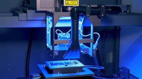
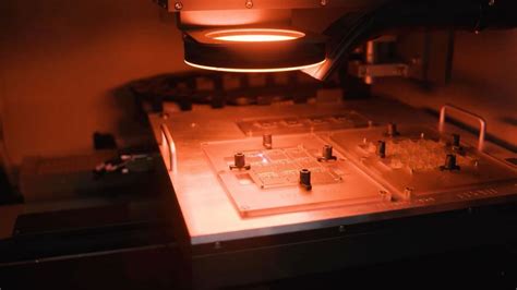
Quality Control Testing Protocols
To ensure reliability in PCB manufacturing, rigorous testing protocols are non-negotiable. Leading PCB manufacturing companies implement automated optical inspection (AOI) to detect microscopic defects in trace alignment, followed by X-ray imaging to verify buried via integrity in multilayer stacks. Electrical testing, including flying probe and boundary scan, validates circuit continuity, while thermal stress simulations assess performance under extreme conditions.
Balancing PCB manufacturing cost with quality demands precision—over-testing inflates expenses, while under-testing risks field failures. Reputable providers optimize this balance by prioritizing critical parameters like impedance control (±10%) and solderability checks. Environmental tests, such as thermal cycling and humidity exposure, further ensure compliance with industry standards like IPC-6012.
For a sustainable PCB manufacturing business, traceability systems track every batch through serialized reporting, enabling root-cause analysis if anomalies arise. By integrating these protocols early in production, you mitigate rework costs and uphold end-product reliability—a cornerstone for high-performance electronics. This systematic approach aligns with broader strategies like rigid-flex design optimization and material selection, ensuring seamless interoperability across all manufacturing stages.
High-Density Interconnect Techniques
When designing complex electronics, PCB manufacturing demands advanced solutions to accommodate shrinking form factors and higher performance requirements. High-density interconnect (HDI) techniques address these challenges by enabling finer traces, smaller vias, and tighter spacing between components. By leveraging laser-drilled microvias (≤100µm) and staggered or stacked via structures, PCB manufacturing companies can achieve up to 20% greater routing density compared to traditional multilayer boards. This precision reduces signal loss while supporting high-speed applications like 5G modules or IoT devices.
A critical consideration in HDI design is balancing PCB manufacturing cost with technical feasibility. While sequential lamination processes and specialized materials increase upfront expenses, they minimize layer counts and overall board size—lowering long-term assembly costs. For instance, using blind/buried vias eliminates redundant through-holes, preserving space for additional circuitry. However, achieving consistent results requires rigorous process controls, such as automated optical inspection (AOI) and impedance testing, to ensure reliability in mission-critical systems.
For PCB manufacturing business leaders, adopting HDI capabilities strengthens competitiveness in aerospace, medical, and automotive markets. Pairing these techniques with embedded passive components or hybrid rigid-flex designs further optimizes performance, making it a strategic investment for next-generation electronics.
Conclusion
When navigating the complexities of PCB manufacturing, your choice of PCB manufacturing companies directly impacts product reliability and performance. Selecting a partner with expertise in high-layer-count designs and advanced processes ensures your boards meet stringent technical demands while optimizing PCB manufacturing cost. From FR-4 substrate optimization to buried copper integration, every decision influences both functionality and scalability in the PCB manufacturing business.
By prioritizing suppliers with robust quality control protocols and flexible production capabilities, you secure alignment with evolving industry standards. Whether balancing rigid-flex design trade-offs or evaluating surface finish durability, understanding these variables empowers smarter investments in multilayer solutions. Ultimately, the right manufacturer becomes a strategic ally, enabling innovation without compromising efficiency or long-term value.
FAQs
How does layer count affect performance in multilayer PCB manufacturing?
The number of layers directly impacts signal integrity, thermal management, and circuit density. PCB manufacturing companies optimize layer stackups to balance cost and performance—higher layer counts (e.g., 12-30 layers) suit complex designs but increase PCB manufacturing cost, while 4-8 layers offer cost efficiency for mid-range applications.
What factors influence material selection for multilayer PCBs?
FR-4 substrates dominate due to their balance of durability and affordability. However, specialized applications may require high-frequency laminates or rigid-flex materials. PCB manufacturing experts assess thermal, mechanical, and electrical requirements to ensure compatibility with your design’s operational demands.
How do surface finishes like Immersion Gold or HASL impact reliability?
Immersion Gold provides superior oxidation resistance and solderability for fine-pitch components, ideal for high-reliability electronics. HASL, while cost-effective, suits applications with larger components. Your choice depends on PCB manufacturing business priorities—durability versus budget constraints.
Why is quality control critical in high-density interconnect (HDI) designs?
HDI circuits demand precision in via formation and trace alignment. Advanced PCB manufacturing processes combine automated optical inspection (AOI) and impedance testing to detect micro-defects, ensuring compliance with aerospace or medical industry standards.
Explore Our Advanced PCB Manufacturing Solutions
For tailored multilayer PCB fabrication, please click here to consult with engineers specializing in optimizing PCB manufacturing cost and performance for your project.


