Precision One Stop PCB Assembly for Complex Projects

Key Takeaways
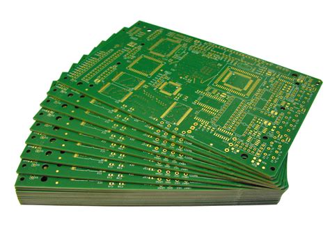
Modern PCB assembly processes have evolved to address intricate design challenges, particularly for projects requiring multilayer boards or high-density interconnects. By leveraging PCBA (Printed Circuit Board Assembly) expertise, engineers can bridge the gap between conceptual designs and functional prototypes, ensuring seamless integration of components like microcontrollers and surface-mount devices.
A critical advantage of integrated services lies in their ability to consolidate design validation, component sourcing, and automated assembly into a unified workflow. For instance:
| Phase | Traditional Approach | One-Stop PCBA Solution |
|---|---|---|
| Design Review | Multiple vendor coordination | Single-point technical oversight |
| Prototyping | 2-4 week lead time | <7-day rapid iteration |
| Quality Assurance | Post-assembly testing | In-process inspection protocols |
This approach not only reduces time-to-market by 30–40% but also minimizes human error through standardized PCB assembly protocols. Advanced methodologies, such as laser-drilled vias and impedance-controlled routing, further enhance reliability for high-frequency applications. Moreover, tailored PCBA solutions adapt to sector-specific needs—whether aerospace-grade thermal management or medical-grade solder masks—ensuring compliance with industry benchmarks without compromising scalability.

Streamline Complex PCB Projects
Managing intricate electronics development requires coordinated integration of PCB assembly processes with design and testing phases. Modern PCBA solutions address this challenge by combining schematic analysis, component sourcing, and automated assembly into a unified workflow. By integrating design validation tools with manufacturing protocols, engineers can identify potential bottlenecks in high-density interconnect (HDI) layouts or mixed-signal configurations before prototyping begins. Advanced PCB assembly platforms utilize machine learning algorithms to optimize trace routing, minimizing signal interference risks in multi-layer boards.
For projects requiring rapid iteration, agile PCBA methodologies synchronize prototype revisions with real-time feedback loops, reducing rework cycles by up to 40%. Automated optical inspection (AOI) systems further streamline quality assurance, cross-referencing 3D board models against physical assemblies to detect micro-scale defects. This holistic approach not only accelerates time-to-market but ensures scalability for transitioning from low-volume batches to full-scale production. Such precision is critical for applications like IoT devices or industrial automation systems, where reliability under extreme conditions directly impacts operational success.
Seamless collaboration between design teams and PCB assembly partners remains pivotal, enabling iterative adjustments to thermal management strategies or EMI shielding requirements without disrupting project timelines.
Precision PCB Assembly Services
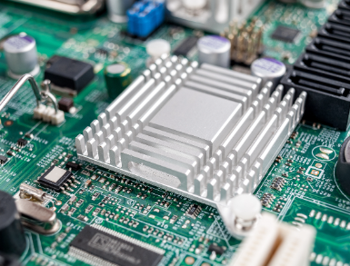
Modern PCB assembly demands meticulous attention to detail, particularly for complex projects requiring high-density interconnects or advanced component integration. Precision PCB assembly (PCBA) services bridge the gap between design intent and functional reality, leveraging cutting-edge equipment like surface-mount technology (SMT) placement systems and automated optical inspection (AOI) tools. These processes ensure components are positioned with micron-level accuracy, minimizing signal interference and thermal inefficiencies.
Tip: When selecting a PCBA partner, verify their capability to handle fine-pitch components (e.g., 0.4mm BGA packages) and mixed-technology boards, as these are critical for advanced applications.
A robust PCB assembly workflow integrates rigorous testing protocols, including in-circuit testing (ICT) and functional validation, to identify flaws before mass production. This is especially vital for industries like aerospace or medical devices, where reliability directly impacts safety. Additionally, design for manufacturability (DFM) feedback during prototyping phases can preempt costly revisions, ensuring seamless scalability from low-volume batches to full-scale runs.
By combining precision engineering with end-to-end traceability, specialized PCBA providers deliver consistent quality across complex projects. This approach not only accelerates time-to-market but also aligns with evolving standards for miniaturization and energy efficiency—key drivers in today’s electronics landscape.
Seamless PCB Assembly Solutions
Modern PCB assembly processes thrive on eliminating friction between design and production phases. By integrating design validation, prototyping, and PCBA manufacturing under a unified workflow, complex projects benefit from synchronized execution. Advanced surface-mount technology (SMT) and through-hole assembly techniques ensure components are placed with micron-level accuracy, minimizing errors during high-volume production.
A key advantage of seamless solutions lies in their adaptability. Whether handling multilayer boards or mixed-technology designs, PCB assembly providers employ automated optical inspection (AOI) and X-ray testing to maintain consistency across batches. Real-time communication between engineers and manufacturers further reduces turnaround times, enabling rapid iterations without compromising quality.
For industries like aerospace or medical electronics, where reliability is non-negotiable, PCBA workflows incorporate traceability systems to monitor every stage—from solder paste application to final functional testing. This end-to-end visibility not only accelerates time-to-market but also aligns with stringent regulatory standards.
By merging expertise in PCB assembly with agile project management, seamless solutions address both technical and logistical challenges. Cross-functional teams collaborate to optimize material sourcing, thermal management, and signal integrity, ensuring prototypes transition smoothly into scalable production. Such integration is critical for projects demanding zero-defect outcomes while navigating tight deadlines.

Advanced PCB Assembly Methods
Modern PCB assembly processes leverage cutting-edge technologies to address the demands of intricate circuit designs. Automated optical inspection (AOI) systems, for instance, enable real-time defect detection during PCBA manufacturing, minimizing errors in high-density interconnect (HDI) boards. Advanced surface-mount technology (SMT) ensures precise component placement, even for micro-BGA and QFN packages, while reflow soldering techniques maintain thermal profiles critical for lead-free alloys. For multilayer designs, laser-drilled vias and controlled impedance routing enhance signal integrity, particularly in high-frequency applications. Additionally, design for manufacturability (DFM) analysis is integrated early in the PCB assembly workflow to preemptively resolve layout conflicts, reducing prototyping iterations. These methodologies, combined with IoT-enabled production monitoring, allow manufacturers to scale complex projects without compromising on PCBA reliability or turnaround times. By harmonizing precision engineering with agile workflows, advanced assembly methods bridge the gap between prototype validation and full-scale production, aligning with the evolving needs of aerospace, medical, and industrial electronics sectors.
Expert Prototyping and Production
PCB assembly transitions from concept to reality through precision-driven prototyping, a critical phase where design flaws are identified and resolved before full-scale manufacturing. Advanced PCBA providers leverage automated pick-and-place systems and 3D solder paste inspection to ensure prototypes mirror final product specifications with micron-level accuracy. This stage enables engineers to test thermal management, signal integrity, and component compatibility under real-world operating conditions.
Seamless scaling from prototype to mass production relies on unified process controls, where data-driven workflows minimize deviations between batches. Certified PCB assembly partners employ traceable material tracking and ISO-certified quality gates, ensuring compliance with IPC-A-610 and J-STD-001 standards. For complex multilayer boards or mixed-technology assemblies, expert coordination between SMT (surface-mount technology) and through-hole processes prevents yield loss during high-volume runs.
By integrating prototyping expertise with production-grade infrastructure, manufacturers eliminate transitional bottlenecks, delivering functional boards that meet both technical benchmarks and accelerated timelines. This synergy is particularly vital for industries requiring mission-critical reliability, such as aerospace or medical device development, where iterative validation directly impacts end-product performance.
Quality-Focused PCB Assembly
In PCB assembly processes, maintaining rigorous quality standards is paramount for ensuring the reliability of complex electronics. Advanced PCBA workflows incorporate automated optical inspection (AOI) and X-ray testing to detect microscopic defects, from solder joint irregularities to component misalignments. These protocols align with ISO 9001 and IPC-A-610 benchmarks, guaranteeing that every board meets both functional and durability requirements.
To address evolving project demands, leading providers integrate traceability systems that monitor each stage of PCB assembly, enabling rapid root-cause analysis for any anomalies. This approach minimizes production delays while upholding consistency across high-volume batches. Additionally, material selection plays a critical role—high-temperature substrates and lead-free solders are prioritized to enhance thermal stress resilience in mission-critical applications.
By embedding quality checks into design validation phases, manufacturers preemptively resolve potential flaws, reducing post-production rework. This proactive strategy not only accelerates time-to-market but also ensures that PCBA outputs align precisely with schematic tolerances. For industries like aerospace or medical devices, where component failure carries significant risks, such meticulous attention to detail transforms PCB assembly from a manufacturing step into a cornerstone of product integrity.
Optimizing Electronics Efficiency
Modern electronics demand PCB assembly processes that maximize operational efficiency while minimizing resource waste. Advanced PCBA methodologies now incorporate automated optical inspection (AOI) systems and real-time performance analytics, enabling engineers to identify bottlenecks in circuit layouts during early prototyping phases. By integrating design validation with manufacturing workflows, holistic optimization addresses both power consumption and signal integrity—critical factors for high-density boards in IoT devices or industrial automation systems.
Transitioning from prototype to mass production requires seamless synchronization between component sourcing and assembly timelines. Leading PCB assembly providers employ Just-In-Time (JIT) inventory models paired with AI-driven demand forecasting, reducing material surplus by up to 30% without compromising production schedules. This approach not only accelerates time-to-market but also aligns with sustainability goals through minimized scrap rates.
For mission-critical applications, precision-tuned PCBA processes leverage impedance-controlled routing and thermal management simulations. These techniques ensure stable performance under extreme operating conditions while maintaining compliance with IPC-A-610 standards. By unifying design analysis, prototyping, and scalable manufacturing under a single workflow, complex projects achieve uninterrupted efficiency gains—from initial concept validation to final quality assurance audits.
Tailored PCB Assembly Services
Modern electronics demand solutions that adapt to unique technical specifications and production timelines. PCB assembly services that prioritize customization enable engineers to address high-density interconnects, mixed-technology boards, and specialized material requirements without compromising performance. Unlike generic approaches, tailored PCBA workflows incorporate dynamic design-for-manufacturing (DFM) analysis, ensuring compatibility with advanced components like BGA packages or embedded systems.
By aligning PCB assembly processes with project-specific parameters, manufacturers can optimize thermal management strategies, impedance control, and signal integrity protocols. This customization extends to batch flexibility, supporting everything from low-volume prototyping to accelerated mass production scaling. Critical industries—including aerospace, medical devices, and industrial automation—leverage these adaptive services to meet stringent regulatory standards while maintaining cost efficiency.
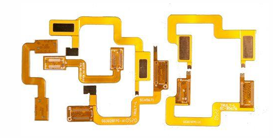
Integrated testing protocols further enhance tailored solutions, with in-line AOI (Automated Optical Inspection) and X-ray verification validating complex assemblies at each stage. Such precision reduces time-to-market risks for innovative products, particularly those requiring rigid-flex configurations or hybrid surface-mount technologies. As project complexities grow, the ability to refine PCBA workflows around evolving technical demands becomes a cornerstone of successful electronics development.
Conclusion
In addressing the demands of modern electronics development, PCB assembly services stand as a cornerstone for bridging innovation with execution. By integrating design validation, prototyping, and full-scale production under a unified workflow, PCBA solutions eliminate fragmented processes that often delay time-sensitive projects. This holistic approach ensures that complex circuit board requirements—from high-density interconnects to mixed-technology components—are managed with technical precision and rigorous quality control.
The value of a one-stop PCB assembly provider lies in its ability to adapt to evolving project needs while maintaining consistency across batches. Whether scaling prototypes into mass production or troubleshooting design iterations, expertise in PCBA translates into reduced risk and enhanced reliability. Advanced methodologies, such as automated optical inspection and functional testing, further safeguard against defects, ensuring compliance with industry standards.
Ultimately, partnering with a service that specializes in PCB assembly empowers engineers to focus on innovation rather than logistical challenges. By leveraging tailored solutions that prioritize both efficiency and accuracy, businesses can accelerate product development cycles while meeting the exacting demands of today’s electronics landscape.

FAQs
What distinguishes one-stop PCB assembly from traditional manufacturing approaches?
A one-stop PCB assembly service integrates design validation, prototyping, and full-scale PCBA production under a single provider, eliminating logistical delays. This approach ensures consistency across stages, particularly for high-complexity projects requiring tight tolerances or advanced materials.
How does prototyping enhance the final PCB assembly outcome?
Prototyping identifies design flaws early, reducing costly revisions during mass production. Expert PCBA teams use this phase to test thermal management and signal integrity, ensuring the final product meets industry-specific standards for reliability.
Can one-stop services handle mixed-technology boards (SMT + through-hole)?
Yes, advanced PCB assembly providers combine automated SMT lines with manual through-hole insertion, accommodating hybrid designs. This flexibility is critical for custom applications like industrial controls or medical devices.
What file formats are required for initiating a PCBA project?
Providers typically require Gerber files (PCB layout), a Bill of Materials (BOM), and a pick-and-place file. For assembly validation, a detailed schematic and testing protocol ensure alignment with functional requirements.
How do quality checks integrate into the assembly workflow?
Automated optical inspection (AOI) and in-circuit testing (ICT) are embedded at critical stages, from prototype PCBA to final units. This multi-layered scrutiny minimizes defects, even in high-density interconnect (HDI) designs.
Optimize Your Next PCB Project Today
Streamline complex builds with end-to-end expertise. Explore our integrated PCB assembly solutions—please click here to discuss your project requirements.