Precision PCB Assembly Solutions for Advanced Electronics
Key Takeaways
When selecting PCB assembly solutions for advanced electronics, prioritizing precision and reliability is paramount. Modern PCBA processes integrate automated optical inspection (AOI) and 3D solder paste inspection (SPI) to ensure flawless component placement, particularly for aerospace, medical, and industrial applications. These sectors demand adherence to IPC-A-610 and ISO 13485 standards, which govern assembly quality and traceability.
Central to high-reliability PCB assembly is the use of advanced materials, such as high-temperature laminates and lead-free solders, engineered to withstand extreme environments. For mission-critical systems, thermal management and signal integrity optimization are non-negotiable, requiring iterative testing protocols like in-circuit testing (ICT) and functional validation.
Moreover, seamless integration of PCBA into complex projects hinges on collaborative design-for-manufacturing (DFM) practices. By leveraging flex-rigid hybrid designs and embedded component technology, manufacturers reduce footprint while enhancing performance—a critical advantage for compact medical devices or avionics systems. Transitioning to scalable production further ensures consistency across low- to high-volume batches, aligning with evolving industry demands.
Precision PCB Assembly for Advanced Electronics
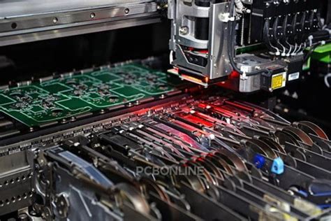
Modern PCB assembly processes demand meticulous attention to detail, particularly for advanced electronics requiring sub-millimeter accuracy. Specialized PCBA workflows leverage automated optical inspection (AOI) and X-ray verification to ensure flawless component placement, even on ultra-thin or flexible substrates. These techniques are critical for applications where signal integrity and thermal management directly impact performance, such as in high-frequency communication modules or embedded control systems.
Tip: When selecting a PCB assembly partner, verify their capability to handle lead-free soldering and mixed-technology boards—both essential for compliance with international safety and environmental standards.
Advanced PCBA solutions integrate 3D solder paste inspection (SPI) and laser-assisted alignment to mitigate defects in high-density designs. This precision is particularly vital for industries like aerospace, where vibration resistance and extended temperature tolerances (-55°C to 150°C) are non-negotiable. For medical devices, biocompatible conformal coatings and hermetic sealing techniques ensure reliability in sterile environments.
"A robust PCB assembly strategy balances design complexity with manufacturability. Prototyping with design-for-manufacturing (DFM) analysis early in development reduces costly revisions."
By combining IoT-enabled traceability with statistical process control (SPC), manufacturers achieve near-zero defect rates in PCBA production. This approach supports seamless integration of multi-layer rigid-flex boards and embedded passive components, enabling next-generation electronics to meet both performance benchmarks and accelerated time-to-market demands.
Cutting-Edge PCB Assembly Technology Solutions
Modern PCB assembly processes leverage automated optical inspection (AOI) and 3D solder paste inspection (SPI) to ensure micron-level accuracy, particularly for high-density interconnect (HDI) designs. These technologies enable PCBA providers to address challenges in miniaturization and signal integrity for advanced electronics, from aerospace avionics to implantable medical devices. By integrating machine learning algorithms into production workflows, manufacturers can predict and mitigate potential defects, reducing rework rates by up to 40% in multi-layer assemblies.
The adoption of laser-direct imaging (LDI) and sequential lamination techniques further enhances precision, allowing for tighter tolerances in complex projects requiring impedance control or RF shielding. For industries like industrial automation, where PCB assembly must withstand extreme temperatures and vibrations, advanced thermal management strategies—such as embedded copper substrates—ensure long-term reliability.
Transitioning to next-gen applications, PCBA specialists now utilize additive manufacturing for rapid prototyping of flexible circuits, accelerating development cycles for IoT and wearable technologies. This focus on innovation not only streamlines production but also aligns with the growing demand for scalable, eco-conscious manufacturing—a critical bridge to the subsequent discussion on high-reliability solutions for mission-critical systems.
High-Reliability PCB Assembly for Critical Systems
In industries where system failures can lead to catastrophic outcomes, PCB assembly processes must adhere to uncompromising standards. High-reliability PCBA focuses on ensuring zero-defect manufacturing through rigorous testing protocols, advanced material selection, and precision-driven workflows. For critical applications such as aerospace guidance systems, medical life-support equipment, or industrial automation controls, even minor deviations in component placement or soldering quality can compromise entire operations.
To meet these demands, specialized PCB assembly providers employ automated optical inspection (AOI), X-ray testing, and environmental stress screening (ESS). These techniques validate solder joint integrity, detect micro-cracks, and simulate extreme operating conditions. Additionally, adherence to standards like IPC-A-610 Class 3 and ISO 9001 ensures traceability and consistency across production batches.
| Key Feature | Industry Application | Compliance Standard |
|---|---|---|
| Thermal Management | Aerospace Avionics | MIL-PRF-31032 |
| Redundancy Checks | Medical Imaging Devices | IEC 60601-1 |
| Vibration Resistance | Industrial Robotics | IPC-6012 Class 3 |
By integrating failure mode and effects analysis (FMEA) during design reviews, manufacturers preemptively address potential weaknesses in PCBA layouts. This proactive approach, combined with multi-stage quality audits, ensures that mission-critical systems operate flawlessly under sustained stress. Transitioning from prototyping to full-scale production, suppliers maintain alignment with client-specific reliability benchmarks, reinforcing the seamless integration of complex electronics into high-stakes environments.
Aerospace-Grade PCB Assembly Services
Aerospace applications demand PCB assembly solutions that withstand extreme conditions while maintaining flawless performance. Mission-critical systems in aviation, satellites, and defense technologies require PCBA processes adhering to IPC-A-610 and AS9100 standards, ensuring rigorous testing for thermal resilience, vibration resistance, and electromagnetic compatibility. Advanced techniques like automated optical inspection (AOI) and X-ray verification are integral to detecting micro-defects in high-density interconnect (HDI) boards, which are common in aerospace electronics.
To meet low-outgassing requirements for space environments, specialized materials such as polyimide substrates and lead-free solders are employed. Manufacturers also implement traceability protocols across the PCB assembly lifecycle, from component sourcing to final validation, to comply with aerospace regulatory frameworks. For instance, avionics control units and communication modules rely on PCBA workflows that prioritize signal integrity and long-term reliability, even under prolonged exposure to radiation or temperature fluctuations.
By integrating these practices, aerospace-grade PCB assembly services ensure seamless functionality in applications where failure is not an option, bridging the gap between cutting-edge design and operational safety.
Medical Device PCB Manufacturing Expertise
In the medical field, PCB assembly demands unparalleled precision to meet stringent regulatory standards and ensure patient safety. Specialized medical-grade PCBA requires adherence to ISO 13485 and FDA guidelines, with a focus on traceability, biocompatibility, and long-term reliability. Manufacturers must integrate high-density interconnect (HDI) designs to accommodate miniaturized devices, such as implantable sensors or portable diagnostic equipment, while maintaining signal integrity in electrically noisy environments.
Advanced PCB assembly techniques, including automated optical inspection (AOI) and X-ray testing, are critical for detecting micro-defects in components used in life-critical systems. Materials like polyimide or ceramic substrates are often selected for their thermal stability and resistance to sterilization processes. Collaboration between design engineers and PCBA providers ensures seamless compliance with risk management protocols, from prototyping to full-scale production. This expertise enables the creation of devices that operate flawlessly under extreme conditions, such as MRI compatibility or continuous monitoring applications, reinforcing trust in medical technology advancements.
Seamless PCB Integration for Complex Projects
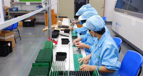
Achieving seamless integration of PCB assembly (PCBA) into multifaceted electronic systems requires meticulous coordination between design, manufacturing, and testing phases. Modern projects in sectors like aerospace, industrial automation, and medical technology demand high-density interconnects, multi-layer configurations, and compatibility with advanced components such as microcontrollers and sensors. Specialized PCBA providers employ automated optical inspection (AOI) and surface-mount technology (SMT) to ensure precise placement of components, minimizing errors in densely packed layouts.
For systems requiring thermal management or signal integrity optimization, embedded trace substrates and rigid-flex PCB designs are often utilized. These techniques enable reliable performance in environments with extreme temperatures, vibrations, or electromagnetic interference. Additionally, design-for-manufacturability (DFM) checks streamline the transition from prototyping to full-scale production, reducing risks of delays in large-scale deployments.
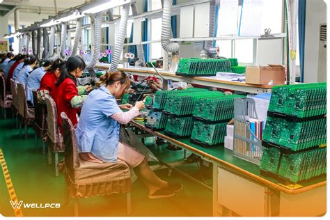
By leveraging PCB assembly expertise, engineers can address challenges like component obsolescence and supply chain variability, ensuring that complex projects meet both functional specifications and regulatory standards. This holistic approach to integration supports scalable solutions, from low-volume custom builds to high-volume automated production, without compromising on precision or reliability.
Advanced PCB Assembly Techniques for Electronics
Modern PCB assembly processes rely on innovative methodologies to meet the demands of high-performance electronics. By integrating automated optical inspection (AOI) and 3D solder paste inspection (SPI), manufacturers ensure micron-level accuracy during PCBA stages, minimizing defects in densely packed circuits. Techniques like laser direct imaging (LDI) enhance trace resolution for high-frequency applications, critical in aerospace and telecommunications systems.
Advanced PCB assembly workflows now incorporate thermo-mechanical simulations to predict stress points in multilayer boards, ensuring long-term reliability under extreme conditions. For medical devices, cleanroom-compliant processes and biocompatible material selection are prioritized to meet stringent regulatory standards. Additionally, PCBA providers utilize mixed-technology assembly, combining surface-mount (SMT) and through-hole components to optimize signal integrity in hybrid designs.
Transitioning from prototyping to mass production, adaptive testing protocols validate performance across environmental variables like temperature fluctuations and vibration. This approach not only aligns with industrial automation requirements but also supports seamless integration into IoT ecosystems. By leveraging these advanced PCB assembly techniques, engineers achieve faster time-to-market while maintaining the precision needed for next-generation electronics.
Optimizing Electronics with Precision Assembly
Achieving peak performance in modern electronic systems hinges on precision PCB assembly processes that balance technical rigor with scalability. Advanced PCBA workflows now integrate automated optical inspection (AOI) systems and laser-aligned pick-and-place machines, ensuring micron-level accuracy for components as small as 01005 packages. This meticulous approach minimizes defect rates while accommodating the dense layouts required for aerospace avionics, medical implants, and industrial IoT devices.
A critical factor in PCB assembly optimization lies in thermal management strategies. High-reliability applications demand precise solder paste application and reflow profiling to prevent thermal stress on sensitive components like BGAs or QFNs. By leveraging data-driven process controls, manufacturers can fine-tune parameters such as solder alloy composition and peak temperatures, ensuring consistent results across high-mix production batches.
Furthermore, PCBA teams are adopting modular design principles to streamline integration with complex subsystems. This includes validating impedance-controlled traces for high-speed signals and implementing conformal coating techniques tailored to harsh operating environments. Such attention to detail not only enhances product longevity but also accelerates time-to-market for mission-critical projects requiring compliance with IPC-A-610 Class 3 or ISO 13485 standards.
Conclusion
In the realm of modern electronics, selecting the right PCB assembly partner is pivotal to achieving uncompromising performance and long-term reliability. As industries such as aerospace, medical, and industrial automation demand increasingly sophisticated solutions, PCBA providers must balance precision engineering with rigorous quality control. The integration of advanced techniques—from automated optical inspection to high-density interconnect (HDI) technologies—ensures that even the most complex designs meet mission-critical standards. By prioritizing PCB assembly processes that emphasize traceability, material integrity, and thermal management, manufacturers can deliver systems capable of withstanding extreme environments and prolonged operational cycles.
For projects requiring seamless collaboration, partnering with a PCBA specialist who understands both the technical and regulatory nuances of your industry becomes indispensable. Whether optimizing signal integrity for aerospace avionics or ensuring biocompatibility in medical devices, the right approach to PCB assembly bridges the gap between innovative design and real-world application. As technology evolves, the ability to adapt and refine these methodologies will remain central to advancing electronics across all sectors.
FAQs
What industries benefit most from precision PCB assembly?
Advanced sectors like aerospace, medical devices, and industrial automation rely on high-precision PCBA solutions. These fields demand strict adherence to performance standards, traceability, and compliance with specialized certifications such as ISO 13485 or AS9100.
How does PCB assembly ensure reliability for critical systems?
Through automated optical inspection (AOI), X-ray testing, and rigorous functional validation, PCBA providers minimize defects. Techniques like conformal coating and thermal management further enhance durability, especially in extreme environments.
What distinguishes aerospace-grade PCBA from standard services?
Aerospace projects require military-grade components, high-Tg laminates, and hermetic sealing to withstand vibration, temperature fluctuations, and radiation. Compliance with MIL-PRF-31032 and IPC-A-610 Class 3 ensures mission-critical reliability.
Why is medical device PCB assembly uniquely challenging?
Biocompatible materials, ultra-clean manufacturing environments, and electromagnetic compatibility (EMC) shielding are essential. Providers must also maintain full traceability for regulatory audits, aligning with FDA 21 CFR Part 820 guidelines.
Can PCB assembly services handle rapid prototyping for complex projects?
Yes, leading PCBA partners offer design-for-manufacturability (DFM) analysis and flexible turnkey solutions, accelerating prototyping without compromising quality. This agility supports iterative testing and scalability for high-volume production.
Explore Customized PCB Assembly Solutions
For tailored PCB assembly services that meet your project’s exact requirements, please click here to consult with our engineering team.


