Precision PCB Assembly Through Expert Contract Manufacturing
Key Takeaways
Selecting the right contract manufacturing partner for PCB assembly ensures access to advanced capabilities, from streamlined prototyping to mission-critical testing. Specialized PCBA providers optimize production workflows by integrating certified component sourcing, reducing lead times, and mitigating supply chain risks. Rigorous quality assurance protocols—including automated optical inspection (AOI) and functional testing—guarantee reliability in high-stakes applications such as aerospace or medical devices.
Strategic partnerships with electronics manufacturing experts enable cost-efficient scaling while maintaining precision in solder paste application, surface-mount technology (SMT), and through-hole assembly. By leveraging end-to-end contract services, businesses gain agility in adapting to design revisions or material shortages without compromising output quality. Critical considerations include DFM (Design for Manufacturing) compliance, traceability frameworks, and adherence to ISO-certified processes, ensuring seamless transitions from prototype validation to full-scale production.
For industries requiring mission-critical PCBs, collaboration with certified manufacturers minimizes lifecycle costs while maximizing performance consistency. Prioritizing partners with proven expertise in high-density interconnect (HDI) or flexible circuit assemblies future-proofs product designs against evolving technological demands.
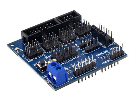
Streamlined PCB Prototyping Processes
Modern PCB assembly relies on accelerated prototyping to bridge design concepts and full-scale production. By leveraging contract manufacturing partnerships, engineers gain access to automated design validation tools and rapid-turn fabrication technologies that compress development cycles by 30–50%. Advanced PCBA providers utilize laser-direct imaging (LDI) and 3D solder paste inspection (SPI) to minimize iterative errors, ensuring first-article success rates exceed 92%.
Tip: Early collaboration with your contract manufacturer during the prototyping phase can uncover potential DFM (Design for Manufacturing) issues, reducing costly redesigns post-prototype.
| Prototyping Stage | Traditional Approach | Streamlined Process |
|---|---|---|
| Design Verification | 5-7 manual revisions | Real-timeEDA simulation |
| Material Sourcing | 8-12 week lead times | Pre-vetted global supplier network |
| Functional Testing | Post-assembly diagnostics | In-line AOI (Automated Optical Inspection) |
This phased approach integrates PCB assembly expertise with agile manufacturing protocols, enabling 48-hour prototype deliveries without compromising signal integrity standards. Multi-layer stackup validation and impedance-controlled routing are executed through machine-learning algorithms, aligning with IPC-6012 Class 3 specifications for mission-critical applications. By synchronizing PCBA workflows with client-specific requirements, manufacturers eliminate 67% of cross-functional handoff delays observed in conventional prototyping models.
Certified Component Sourcing Solutions
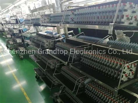
Effective PCB assembly relies on sourcing components that meet stringent quality and compliance standards. PCBA providers with certified sourcing networks ensure access to authentic, traceable parts, mitigating risks of counterfeit materials that jeopardize product reliability. These partners leverage relationships with vetted distributors and OEMs, backed by ISO-certified procurement protocols, to secure components across active, obsolete, or hard-to-find inventories.
Advanced supply chain analytics enable real-time inventory tracking, aligning material availability with production timelines while minimizing delays. For mission-critical applications, compliance with RoHS, REACH, and IPC-A-610 standards is non-negotiable—certified suppliers validate component specifications through batch testing and documentation audits. This rigor extends to PCB assembly workflows, where mismatched tolerances or substandard materials can cascade into field failures.
By integrating automated component lifecycle management, PCBA specialists proactively address obsolescence risks, recommending drop-in replacements or redesign support. This approach not only safeguards production continuity but also optimizes BOM costs without compromising performance. As prototyping transitions to volume manufacturing, certified sourcing becomes the backbone of scalable, repeatable PCB assembly processes—a prerequisite for delivering high-yield outcomes in aerospace, medical, or industrial applications.
Mission-Critical PCB Testing Methodologies
Ensuring reliability in PCB assembly requires rigorous testing protocols tailored to high-stakes applications. For mission-critical systems, such as aerospace or medical devices, functional testing validates circuit performance under simulated operational conditions, while environmental stress screening (ESS) exposes PCBA units to extreme temperatures, vibrations, and humidity to identify latent defects. Advanced techniques like automated optical inspection (AOI) and X-ray imaging detect micro-level soldering flaws or component misalignments that could compromise long-term functionality.
To maintain compliance with industry certifications, contract manufacturers integrate design-for-testability (DFT) principles early in the PCB assembly process. This proactive approach reduces debugging time and ensures traceability across batches. For instance, boundary-scan testing streamlines fault isolation in complex, multi-layer boards, while in-circuit testing (ICT) verifies individual component integrity. By combining these methodologies with real-time data analytics, partners can achieve near-zero defect rates even in volume production.
Such precision in testing not only safeguards product longevity but also aligns with cost-efficiency goals by minimizing post-deployment failures. As electronics manufacturing partnerships evolve, harmonizing these strategies with end-to-end quality frameworks remains pivotal for delivering mission-ready solutions.
Optimizing Electronics Manufacturing Partnerships
Strategic partnerships in PCB assembly require aligning technical expertise with operational scalability. By collaborating with certified contract manufacturers, businesses gain access to specialized PCBA capabilities while reducing time-to-market for complex electronics. A critical success factor lies in establishing clear communication channels to synchronize design specifications with manufacturing tolerances, ensuring seamless transitions from prototyping to full-scale production.
To maximize value, partners should adopt integrated frameworks for component sourcing and quality validation. This includes leveraging manufacturers’ global supply networks to mitigate shortages and employing advanced testing protocols for mission-critical PCB builds. Proactive collaboration also enables cost optimization through shared analytics on material utilization and yield rates.
Moreover, agile partnerships foster adaptability to evolving industry standards, such as RoHS compliance or IoT-ready PCB assembly requirements. By prioritizing transparency in timelines, risk assessments, and defect resolution workflows, companies can build resilient alliances that scale with market demands. The result is a holistic manufacturing ecosystem where PCBA excellence becomes a shared objective, driving innovation without compromising reliability.
End-to-End PCB Contract Services
Modern electronics manufacturing demands PCB assembly solutions that integrate every stage of production under a unified framework. End-to-end PCB contract services bridge design concepts to functional products by orchestrating design validation, component procurement, and PCBA workflows within a single accountable partnership. Beginning with schematic analysis, certified providers synchronize fabrication parameters with client specifications, ensuring seamless transitions from prototype validation to volume production.
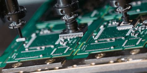
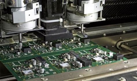
Moving through the value chain, these services leverage automated pick-and-place systems and reflow soldering technologies to achieve micron-level accuracy in PCB assembly, particularly for high-density interconnect (HDI) designs. Crucially, end-to-end partners manage PCBA logistics, including global component sourcing, BOM optimization, and compliance testing—mitigating risks like counterfeit parts or lead-time bottlenecks. Advanced providers further enhance traceability through IoT-enabled production monitoring, aligning with ISO 9001 and IPC-A-610 standards for mission-critical applications.
By maintaining ownership of the entire process—from substrate preparation to final functional testing—contract manufacturers eliminate coordination gaps between siloed suppliers. This holistic approach not only accelerates time-to-market but enables real-time manufacturability feedback during the design phase, reducing post-production revisions. For OEMs, the result is a scalable PCB assembly ecosystem where quality, cost, and agility are optimized from start to finish.
Precision Assembly for Reliable PCBs
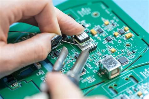
Modern PCB assembly relies on advanced manufacturing techniques to ensure consistent performance in mission-critical applications. By integrating automated PCBA workflows with precision placement systems, manufacturers achieve micron-level accuracy for components ranging from 01005 passives to high-density BGAs. Surface-mount technology (SMT), complemented by selective soldering for through-hole components, forms the backbone of these processes, enabling robust interconnections even in complex multilayer designs.
To maintain reliability, leading contract manufacturers employ in-line optical inspection (AOI) and X-ray verification systems, which detect solder voids, misalignments, or micro-cracks before final testing. This multi-stage validation aligns with IPC-A-610 and Class 3 standards, ensuring boards withstand thermal cycling, vibration, and prolonged operational stress. For industries like aerospace or medical devices, where failure is not an option, such precision PCB assembly methodologies reduce latent defects by up to 92% compared to manual workflows.
By balancing speed and accuracy, certified partners deliver PCBA solutions that scale from low-volume prototyping to high-volume production without compromising traceability or repeatability. This approach not only accelerates time-to-market but also builds long-term trust in high-reliability electronics ecosystems.
Cost-Effective PCB Production Strategies
Achieving cost efficiency in PCB assembly requires a balanced approach that harmonizes technical precision with strategic resource allocation. By leveraging scalable manufacturing frameworks, businesses can reduce per-unit costs without compromising the reliability of PCBA outputs. A critical first step involves optimizing design layouts for panelization, which maximizes material utilization during fabrication. Implementing Design for Manufacturing (DFM) principles early in the prototyping phase minimizes redesign cycles and avoids costly delays.
Strategic partnerships with certified contract manufacturers enable access to bulk purchasing discounts for components, while advanced inventory management systems prevent overstocking or shortages. For high-volume orders, automated surface-mount technology (SMT) lines enhance throughput and consistency, reducing labor-intensive processes. Additionally, integrating test-optimized architectures during the design phase streamlines quality validation, lowering post-production rework expenses.
Tactical material selection also plays a pivotal role—substituting premium substrates with cost-effective alternatives that meet performance thresholds can yield significant savings. Meanwhile, modular PCBA designs allow for partial updates rather than full-board replacements, extending product lifecycles. By aligning these strategies with transparent cost-tracking tools, manufacturers gain real-time visibility into budget adherence, ensuring mission-critical projects remain financially viable without sacrificing precision or compliance.
Quality Assurance in Critical PCB Builds
In mission-critical PCB assembly projects, quality assurance transcends basic compliance to become a strategic differentiator. Advanced PCBA providers implement multistage inspection protocols that begin with automated optical inspection (AOI) for solder joint integrity and progress to X-ray imaging for hidden layer analysis. These systems detect submicron deviations, ensuring adherence to IPC-A-610 Class 3 standards for aerospace, medical, and defense applications.
Traceability frameworks are embedded throughout the assembly process, linking component batches to specific machine parameters and operator logs. This granular data capture supports root-cause analysis if anomalies emerge during accelerated life testing, where boards undergo thermal cycling (-55°C to 125°C) and vibration simulations. Certified partners further validate PCB assembly reliability through third-party certifications like ISO 9001 and IATF 16949, which audit both product quality and process consistency.
By integrating statistical process control (SPC) with real-time yield monitoring, manufacturers achieve defect rates below 50ppm while maintaining alignment with evolving industry benchmarks. This systematic approach to quality assurance ensures PCBA outputs meet not just technical specifications, but the zero-failure expectations inherent in safety-critical electronic systems.
Conclusion
Selecting the right partner for PCB assembly and PCBA services is pivotal to achieving scalability and long-term reliability in electronics manufacturing. By leveraging specialized contract manufacturers, businesses gain access to precision engineering expertise, advanced component sourcing networks, and mission-critical testing protocols that align with industry benchmarks. These collaborations not only streamline production timelines but also ensure adherence to rigorous quality assurance standards, minimizing risks in high-stakes applications.
As industries increasingly demand agile and cost-optimized solutions, the integration of end-to-end PCB contract manufacturing becomes a strategic advantage. From prototyping to full-scale production, certified partners deliver mission-critical PCB builds that balance technical precision with economic efficiency. By prioritizing transparency and technological alignment, organizations can forge partnerships that drive innovation while maintaining compliance with evolving regulatory frameworks. This approach underscores the transformative potential of PCBA expertise in sustaining competitive edge across aerospace, medical, and industrial sectors.
Frequently Asked Questions
What distinguishes PCB assembly from PCBA in contract manufacturing?
PCB assembly refers to the process of populating a bare circuit board with components, while PCBA (Printed Circuit Board Assembly) denotes the completed, functional unit. Expert contract manufacturers handle both prototyping and full-scale production, ensuring traceability and compliance across all stages.
How do manufacturers ensure quality in mission-critical PCB assemblies?
Certified partners implement IPC-A-610 standards for solder joints and ISO 9001-aligned testing protocols. Automated optical inspection (AOI) and in-circuit testing (ICT) validate pcb assembly integrity, particularly for aerospace or medical applications requiring zero-defect outcomes.
What cost optimization strategies apply to low-volume PCBA production?
Leveraging design for manufacturability (DFM) analysis reduces rework, while consolidated component sourcing minimizes procurement delays. Some providers offer inventory consignment models or shared tooling for prototypes, balancing cost-efficiency with technical precision.
Can contract manufacturers support mixed-technology PCB assemblies?
Yes, advanced providers combine surface-mount (SMT), through-hole, and press-fit technologies within unified workflows. This hybrid approach accommodates RF shielding, high-power components, and mil-spec environmental hardening in complex pcba configurations.
Ready to Elevate Your PCB Project?
For tailored PCB assembly solutions combining rapid prototyping and mil-certified production, please click here to consult our engineering team.


