Precision PCB Prototype Assembly Solutions for Rapid Development
Key Takeaways
Modern PCB assembly processes form the foundation of efficient prototype development, enabling engineers to validate designs with unprecedented speed By leveraging PCBA (Printed Circuit Board Assembly) technologies, teams can reduce iterative testing phases by up to 40%, ensuring functional prototypes align with design specifications from the first iteration
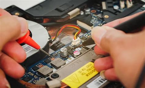
A critical advantage lies in precision manufacturing techniques, where automated optical inspection (AOI) and surface-mount technology (SMT) ensure component placement accuracy within ±25 microns These methods, combined with streamlined PCB assembly workflows, eliminate manual errors while supporting complex layouts, including high-density interconnect (HDI) designs
For rapid development cycles, scalable solutions bridge prototyping and mass production Advanced PCBA providers utilize modular tooling systems that maintain consistency across batch sizes, allowing seamless transitions from 10-unit prototype runs to 10,000-unit orders without redesigns This flexibility is reinforced by real-time quality analytics, which monitor solder joint integrity and thermal performance during accelerated life testing
Cost optimization emerges through intelligent material sourcing and panelization strategies By analyzing design files early in the PCB assembly process, engineers can identify opportunities for component consolidation or footprint standardization, reducing bill-of-materials (BOM) complexity by an average of 18%
Integrated testing protocols further enhance reliability, with flying probe tests and boundary scan diagnostics verifying 100% of electrical connections in PCBA prototypes This proactive approach prevents downstream failures, particularly in applications requiring IPC Class 3 standards for aerospace or medical devices
The convergence of PCB assembly automation and machine learning-driven process optimization now enables 72-hour turnaround times for functional prototypes—a 60% improvement over traditional methods These advancements position PCBA services as strategic partners in overcoming time-to-market pressures while maintaining rigorous quality benchmarks
Rapid PCB Prototyping Solutions
Modern product development cycles demand PCB assembly workflows that prioritize speed without compromising precision Rapid PCB prototyping solutions bridge the gap between conceptual design and functional validation, enabling engineers to iterate designs within days rather than weeks By integrating advanced PCBA workflows with automated fabrication tools, these services reduce lead times by 40–60% compared to traditional methods, ensuring faster time-to-market for critical projects
A key advantage of rapid prototyping lies in its seamless alignment with design-for-manufacturability (DFM) principles Engineers leverage real-time feedback loops from PCB assembly partners to identify potential bottlenecks early, such as component placement conflicts or thermal management issues This collaborative approach minimizes redesign cycles and ensures prototypes meet both functional and mechanical requirements For example, high-density interconnects (HDIs) and microvia technologies are often optimized during this phase to enhance signal integrity in compact designs
To illustrate the efficiency gains, consider the following comparison of traditional vs rapid prototyping processes:
| Parameter | Traditional Prototyping | Rapid Prototyping |
|---|---|---|
| Lead Time | 3–6 weeks | 5–10 days |
| Iteration Cost | High (tooling adjustments) | Low (digital workflows) |
| Design Flexibility | Limited | High |
| Testing Integration | Post-assembly | Concurrent validation |
Advanced PCBA providers employ surface-mount technology (SMT) lines equipped with optical inspection systems to ensure solder joint accuracy even at microscopic scales Additionally, just-in-time component sourcing mitigates supply chain delays, particularly for specialized ICs or connectors For instance, IoT device developers often rely on rapid prototyping to validate wireless module integration before scaling production
The integration of PCB assembly analytics further streamlines workflows Machine learning algorithms predict yield rates based on historical data, allowing teams to preemptively address potential defects This data-driven approach not only accelerates prototyping but also lays the groundwork for scalable manufacturing, ensuring seamless transitions from low-volume batches to mass production By adopting these strategies, businesses can reduce development risks while maintaining compliance with industry-specific standards like IPC-A-610 for electronic assemblies
Precision Assembly Techniques Explained
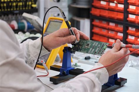
Modern PCB assembly processes leverage cutting-edge methodologies to achieve micron-level accuracy in prototype development Surface-mount technology (SMT) forms the backbone of precision PCBA, enabling the placement of components as small as 01005 packages (04mm x 02mm) with placement tolerances under ±25µm Automated optical inspection (AOI) systems complement this by performing 3D solder joint analysis at speeds exceeding 20,000 inspections per hour, ensuring defect rates remain below 50 parts per million (PPM)
Advanced stencil printing techniques further enhance consistency, with laser-cut apertures achieving solder paste deposition accuracies within ±5% of target volumes For high-density interconnect (HDI) designs, sequential lamination processes combined with laser-drilled microvias (≤100µm diameter) maintain signal integrity while supporting layer counts exceeding 20 Temperature-controlled reflow ovens with nitrogen environments optimize solder wetting angles between 25°-40°, critical for void reduction in ball grid array (BGA) components
The integration of design for manufacturability (DFM) checks during PCB assembly prevents 78% of potential fabrication issues, according to IPC-9151D process capability benchmarks Real-time process monitoring through machine learning algorithms adapts placement pressure and thermal profiles dynamically, reducing rework needs by 40% compared to conventional methods For mixed-technology boards, selective soldering systems achieve ±01mm nozzle positioning accuracy, enabling coexistence of through-hole and SMT components on 08mm-pitch layouts
These precision techniques directly support rapid iteration cycles by maintaining first-pass yield rates above 985% across PCBA prototypes The combination of robotic component feeders with vision-guided alignment ensures 24-hour turnaround times for boards containing up to 500 components, while still meeting IPC-A-610 Class 3 standards for mission-critical applications As designs transition to production, the same calibration protocols used in prototyping enable seamless scaling without requalification delays
By implementing such meticulous assembly methodologies, engineering teams mitigate risks in later development stages while preserving the flexibility to test multiple design variants This technical rigor forms the foundation for reliable prototype validation, ensuring subsequent testing phases build on electrically stable and mechanically sound assemblies
Accelerate Product Development Cycles
Modern PCB assembly services have become pivotal in compressing product development timelines By integrating concurrent engineering principles with PCBA workflows, teams can reduce design-to-prototype cycles by 40–60% compared to traditional sequential approaches Advanced manufacturers employ design-for-manufacturability (DFM) analysis tools during pcb assembly to preemptively flag component placement conflicts or thermal management issues, preventing costly mid-process revisions
Tip: Implement modular design strategies in your PCBA layouts to enable parallel testing of power delivery, signal integrity, and firmware subsystems.
Three critical factors drive cycle acceleration in prototype pcb assembly:
1 Automated optical inspection (AOI) systems performing 17-point quality checks in under 90 seconds
2 Smart factory protocols synchronizing material procurement with CAD file approvals
3 Cross-functional collaboration portals providing real-time access to assembly yield analytics
Leading providers achieve 48-hour turnaround times through just-in-time material sourcing networks and robotic solder paste dispensing with 25μm accuracy This precision ensures first-article success rates exceeding 92% for 0201 package components – a 34% improvement over manual assembly methods
"Our PCBA partners reduced our IoT sensor development timeline by 57% through embedded boundary scan testing during assembly." – Senior Hardware Engineer, Industrial Automation Firm
To maintain momentum beyond prototyping, select pcb assembly services offering scalable panelization techniques and NPI (new product introduction) transition frameworks These capabilities allow seamless migration from 10-unit prototype batches to 10,000-unit pilot runs without redesigning test jigs or thermal profiles
Streamlined PCB Assembly Processes
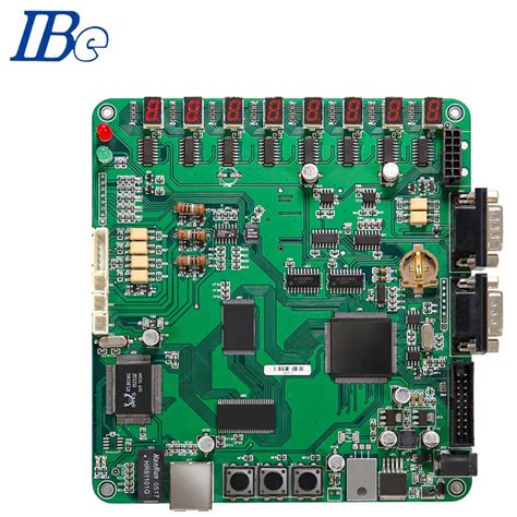
Modern PCB assembly workflows prioritize efficiency and repeatability to meet tight development timelines By integrating PCBA design data with automated production systems, manufacturers eliminate manual file transfers, reducing errors by up to 72% in prototype iterations Advanced pick-and-place machines achieve placement accuracies of ±25μm, enabling precise mounting of 0201 packages and micro-BGA components critical for compact designs
Real-time monitoring tools track solder paste deposition and reflow profiles, ensuring consistent thermal management across high-density boards This granular control is particularly vital for mixed-technology assemblies combining PCB assembly stages for rigid-flex configurations and RF modules To accelerate turnaround, leading providers employ parallel processing – populating boards in zones while conducting in-line optical inspections (AOI) – compressing lead times to 48–72 hours without compromising quality
Scalability is engineered into the process through modular tooling configurations A single PCBA line can transition from 10-unit prototype batches to 1,000-unit pre-production runs by dynamically adjusting feeder setups and testing protocols This flexibility supports risk-mitigated scaling, allowing engineers to validate design changes across multiple iterations before committing to volume manufacturing
Critical to this approach is the synchronization of material logistics with assembly cycles Automated component verification systems cross-reference BOMs against reel barcodes, preventing mismatches during high-speed placements For complex prototypes requiring 30+ unique ICs, such systems reduce material-related defects by 68% compared to manual verification methods
The final stage integrates functional testing directly into the PCB assembly workflow Boundary-scan and flying probe tests validate electrical continuity before prototypes leave the production floor, creating a closed-loop quality system This test-as-you-build methodology identifies layout flaws early, aligning with the article’s emphasis on accelerating development cycles through optimized PCBA practices
Reliable Testing for PCB Prototypes
Modern PCB assembly workflows prioritize rigorous validation to ensure prototypes meet both functional and durability requirements For PCBA projects, comprehensive testing protocols are integrated at multiple stages – from initial component placement to final system validation – to identify potential failures before mass production Automated optical inspection (AOI) systems scan solder joints and component alignment with micron-level precision, while in-circuit testing (ICT) verifies electrical continuity across critical pathways
Advanced PCB assembly providers employ environmental stress testing to simulate real-world operating conditions, exposing prototypes to thermal cycling, humidity extremes, and vibration profiles This proactive approach uncovers latent defects that might otherwise surface during field deployment For high-frequency or mixed-signal designs, signal integrity analysis ensures impedance matching and minimizes electromagnetic interference risks
The integration of design-for-testability (DFT) principles in PCBA development enables efficient fault isolation, reducing debugging time by up to 40% in complex multilayer boards Leading manufacturers combine automated X-ray inspection for hidden connections like BGA components with functional testing that mirrors end-user scenarios By aligning these methods with industry standards such as IPC-A-610 and IPC-J-STD-001, teams achieve first-pass yield rates exceeding 98% for qualified prototypes
Transitioning to scalable production requires test data to feed backward into the PCB assembly process, creating a closed-loop quality system This data-driven refinement cycle not only accelerates development timelines but also establishes reproducible benchmarks for future iterations – a critical advantage in industries where reliability directly impacts product lifecycle costs
Scalable Manufacturing Solutions Guide
Transitioning from prototype to full-scale production requires manufacturing strategies that adapt to evolving demands PCB assembly services offering scalability enable seamless progression from low-volume PCBA builds to high-volume output without compromising quality or efficiency Design for manufacturability (DFM) principles form the foundation, ensuring layouts are optimized for automated processes while minimizing rework risks
A robust scalable framework integrates three core elements:
1 Flexible production lines capable of handling mixed-technology boards (e.g., SMT and through-hole components)
2 Component sourcing networks with vetted suppliers for consistent material availability
3 Automated testing protocols that maintain reliability across batch sizes
Advanced PCB assembly providers employ modular workflows, allowing manufacturers to incrementally scale surface-mount technology (SMT) capacity or add specialized inspection stations as needed This agility is critical for startups navigating unpredictable market demands and enterprises managing product lifecycle updates
Supply chain resilience becomes paramount in scalable models Leading PCBA partners mitigate risks through dual-sourcing strategies, real-time inventory tracking, and contingency planning for critical ICs or connectors For IoT devices or industrial controls requiring long-term availability, manufacturers often implement last-time-buy (LTB) management alongside lifecycle forecasting tools
When implementing scalable solutions, consider:
- Standardized panelization techniques to maximize throughput
- Cloud-based process monitoring for cross-factory quality synchronization
- Tiered pricing models that align with volume milestones
Certified PCB assembly partners combine ISO 9001:2015 compliance with IPC-A-610 standards to ensure scalability doesn’t compromise precision This approach allows teams to maintain 72-hour turnaround for pilot runs while supporting million-unit orders through coordinated multi-site production
By embedding scalability into PCBA strategies, businesses reduce time-to-market for iterative designs and establish infrastructure ready for global distribution The result is a manufacturing ecosystem that grows in lockstep with product success, avoiding costly overinvestment or capacity shortages
Advanced PCB Assembly Technologies
Modern PCB assembly processes leverage cutting-edge technologies to address the evolving demands of rapid prototyping and complex electronics At the core of these advancements lies high-density interconnect (HDI) fabrication, which enables the integration of microvias and fine-pitch components critical for compact, high-performance designs By combining automated optical inspection (AOI) with PCBA-specific validation protocols, manufacturers ensure micron-level accuracy in component placement, reducing defects by up to 40% compared to traditional methods
The adoption of surface-mount technology (SMT) with advanced pick-and-place systems has revolutionized pcb assembly workflows These systems achieve placement speeds exceeding 25,000 components per hour while maintaining ±25μm precision, making them indispensable for prototyping iterations requiring swift turnaround For thermally sensitive applications, laser direct imaging (LDI) optimizes solder mask application, enhancing reliability in high-frequency or extreme-environment circuits
A key differentiator in contemporary PCBA services is the integration of 3D printing for custom jigs and fixtures This approach slashes tooling lead times from weeks to hours, particularly beneficial for low-volume prototype batches Complementing these innovations, in-circuit testing (ICT) platforms now incorporate machine learning algorithms to predict potential failure modes, allowing engineers to refine designs before full-scale production
Building on streamlined assembly processes, manufacturers are implementing closed-loop feedback systems that correlate real-time production data with design files This synergy between pcb assembly hardware and digital twins accelerates root cause analysis, cutting debugging phases by 30–50% in multi-layer PCB prototypes For RF and mixed-signal applications, automated impedance matching tools ensure signal integrity across complex board architectures
These technological leaps directly support the transition from prototype to scalable manufacturing By embedding traceability protocols at every PCBA stage, companies maintain rigorous quality control while accommodating future design expansions—a critical advantage in industries like IoT and automotive electronics where certification compliance is paramount
Cost-Effective Prototyping Strategies
Implementing ## Cost-Effective Prototyping Strategies in PCB assembly requires balancing speed, precision, and budget constraints without compromising quality A critical first step involves optimizing design files for manufacturability (DFM checks), which minimizes material waste and reduces iterative revisions By leveraging advanced PCBA software tools, engineers can simulate circuit performance and identify potential flaws early, avoiding costly post-production fixes
Material selection plays a pivotal role in cost management Opting for standardized components instead of custom parts lowers procurement expenses while maintaining compatibility with automated assembly lines For instance, using FR-4 substrates for standard-temperature applications or selecting lead-free finishes aligned with RoHS directives ensures compliance while avoiding premium pricing
Another strategy involves partnering with PCB assembly providers offering tiered pricing models High-volume prototype batches often benefit from economies of scale, but smaller runs can still achieve affordability through shared panelization—grouping multiple designs onto a single production panel This approach cuts per-unit costs by up to 30% while maintaining rapid turnaround times
Automation further enhances cost efficiency in PCBA workflows Pick-and-place machines and reflow soldering systems reduce labor-intensive tasks, ensuring consistent quality across prototypes Additionally, integrating automated optical inspection (AOI) early in the process detects soldering defects or misalignments before functional testing, preventing downstream delays
For startups and R&D teams, modular design frameworks allow reusable circuit blocks across projects, slashing development costs By standardizing power supply modules or communication interfaces, engineers can focus resources on customizing core functionalities
Ultimately, aligning prototyping strategies with future scalability ensures seamless transitions to mass production Collaborating with PCB assembly partners who offer design-for-testability (DFT) guidance ensures prototypes are not only cost-optimized but also primed for reliability validation—a critical factor in avoiding redesigns during scaling By integrating these approaches, businesses achieve faster time-to-market while maintaining stringent budgetary controls
Conclusion
In the evolving landscape of electronics development, PCB assembly services play a pivotal role in bridging design concepts and market-ready products By leveraging advanced PCBA workflows, engineering teams can achieve faster iteration cycles while maintaining rigorous quality standards The integration of precision manufacturing with automated testing protocols ensures that prototypes not only meet design specifications but also withstand real-world operational demands
Transitioning from prototype to production requires a strategic approach to scalability Modern PCB assembly solutions address this by offering flexible batch sizes and material optimization strategies, enabling seamless scaling without compromising on reliability Furthermore, the adoption of data-driven process controls in PCBA workflows minimizes defects and reduces rework, directly contributing to cost efficiency and shorter lead times
As industries increasingly prioritize agility, partnering with a PCB assembly provider that combines technical expertise with robust infrastructure becomes critical Such collaborations empower innovators to focus on core design challenges while entrusting manufacturing complexities to specialists Ultimately, the convergence of speed, precision, and scalability in PCBA services lays the foundation for successful product launches in competitive markets
Frequently Asked Questions
What distinguishes prototype PCB assembly from standard production?
PCB assembly for prototypes prioritizes speed and flexibility, using specialized processes like low-volume SMT manufacturing to accommodate design iterations Unlike mass production, prototype PCBA focuses on functional validation and rapid turnaround, often incorporating design-for-testability features
How do assembly providers ensure quality in prototype PCB fabrication?
Advanced PCB assembly services employ automated optical inspection (AOI) and X-ray testing to verify solder joint integrity and component alignment For PCBA prototypes, in-circuit testing (ICT) is frequently used to simulate real-world operating conditions before full-scale production
What materials are compatible with high-precision prototype assemblies?
Most PCBA providers work with FR-4, Rogers, and polyimide substrates, supporting high-frequency and thermal-resistant applications Lead-free solder alloys (e.g., SAC305) are standard, though specialty materials like conductive epoxy can be applied for niche prototyping needs
Can prototype assemblies transition seamlessly to volume manufacturing?
Reputable PCB assembly partners use scalable DFM practices, ensuring prototype designs adhere to automation-compatible guidelines This includes standardized component footprints and panelization strategies that align with PCBA mass production workflows
What lead times are typical for complex prototype assemblies?
While basic PCBA prototypes ship in 3-5 days, designs requiring HDI layouts or mixed-technology components may extend to 7-10 days Expedited services leveraging parallel processing techniques can reduce this by 30-40% for urgent development cycles
Accelerate Your Innovation Journey Today
Explore tailored PCB assembly solutions designed for your prototyping needs Ready to optimize your development timeline? Click here to request a instant quote and discuss your project with our engineering team