Precision Wiring in Amplifier PCB Design: Techniques and Best Practices
Introduction
Printed Circuit Board (PCB) design for audio amplifiers requires meticulous attention to wiring precision to ensure optimal signal integrity, minimize noise, and maintain the amplifier’s performance characteristics. The quality of an amplifier’s sound reproduction is directly influenced by how effectively the PCB layout manages signal paths, power distribution, and grounding schemes. This article explores the fundamental principles and advanced techniques for achieving precise wiring in amplifier PCB designs.
Understanding the Importance of Precision in Amplifier PCBs
Audio amplifier circuits are particularly sensitive to layout imperfections due to several factors:
- High Gain Requirements: Small signals at the input get amplified significantly, making them vulnerable to noise pickup.
- Wide Frequency Response: Audio amplifiers must handle frequencies from 20Hz to 20kHz (or beyond for some designs), requiring careful consideration of impedance and parasitic effects.
- Mixed Signal Environment: Combining low-level analog signals with high-current power stages creates challenging layout scenarios.
- Thermal Considerations: Power dissipation in output stages can affect component performance and reliability.
Precision in PCB wiring addresses these challenges by:
- Minimizing parasitic capacitance and inductance
- Reducing electromagnetic interference (EMI)
- Optimizing thermal management
- Maintaining signal integrity throughout the audio band
Fundamental Principles of Precision Wiring
1. Signal Flow Optimization
The golden rule of amplifier PCB layout is to follow the signal path logically from input to output:
- Input Stage: Place input connectors and components close to the amplifier’s input section. Keep input traces as short as possible to minimize noise pickup.
- Gain Stages: Arrange amplification stages sequentially, avoiding crossed or looping traces.
- Output Stage: Position output transistors or ICs near the output connectors with appropriate trace widths for current handling.
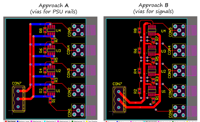
2. Grounding Strategies
Proper grounding is perhaps the most critical aspect of amplifier PCB design:
- Star Grounding: Create a single-point ground connection where all ground returns meet, typically near the power supply filter capacitors.
- Separate Ground Planes: Consider separate analog and power ground planes connected at a single point for mixed-signal designs.
- Ground Trace Width: Ensure ground traces are sufficiently wide (often 2-3 times wider than signal traces) to handle return currents.
3. Power Distribution
- Decoupling Capacitors: Place decoupling capacitors as close as possible to active devices (ICs, transistors).
- Power Trace Sizing: Calculate appropriate trace widths based on current requirements (using IPC-2221 standards or online calculators).
- Power Plane Usage: For complex designs, dedicate entire layers to power distribution when possible.
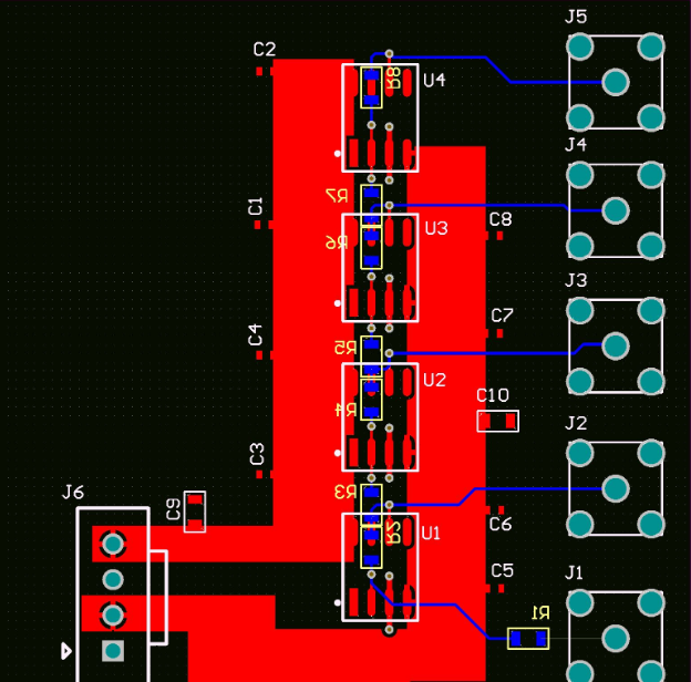
4. Component Placement
Strategic component placement facilitates precise wiring:
- Group Related Components: Keep components of each functional block (input stage, voltage amplification, output stage) in close proximity.
- Orientation: Align components in consistent directions to simplify routing.
- Thermal Considerations: Position heat-generating components with adequate spacing and thermal relief.
Advanced Precision Wiring Techniques
1. Controlled Impedance Routing
For high-frequency stability in wideband amplifiers:
- Calculate trace impedance based on dielectric thickness and trace width
- Maintain consistent impedance along critical signal paths
- Use microstrip or stripline configurations where appropriate
2. Differential Pair Routing
For balanced input stages or differential amplifier sections:
- Route differential pairs as close together as possible
- Maintain equal trace lengths to preserve signal timing
- Use curved traces rather than 90° angles to minimize impedance variations
3. Shielding Techniques
- Implement guard rings around sensitive high-impedance nodes
- Use grounded copper pours between critical traces
- Consider shielded cables or connectors for off-board connections
4. Thermal Management Through Layout
- Use thermal vias under power devices to transfer heat to opposite layers
- Incorporate copper pours as heat sinks for power components
- Position temperature-sensitive components away from heat sources
Practical Implementation Steps
1. Schematic Preparation
- Hierarchical Design: Break the amplifier into functional blocks (power supply, input stage, output stage)
- Net Labeling: Clearly label critical nets (e.g., “SIGNAL_IN”, “PWR_RAIL”)
- Component Footprints: Verify physical dimensions match schematic symbols
2. Board Outline Definition
- Mechanical Constraints: Account for enclosure requirements, heatsinks, and connectors
- Layer Stackup: Determine appropriate number of layers based on complexity
- Keepout Areas: Identify restricted zones for mounting or thermal considerations
3. Component Placement
- Critical Path First: Place input components, then amplification stages, followed by output devices
- Power Components: Position transformers, large capacitors, and regulators considering weight distribution
- Connector Placement: Align I/O connectors with enclosure requirements
4. Routing Execution
- Critical Signals First: Route sensitive audio paths before less critical connections
- Power Routing: Implement power distribution with adequate trace widths
- Grounding: Establish solid ground return paths
- Crossing Prevention: Avoid having signal traces cross split ground planes
5. Verification and Optimization
- Design Rule Check (DRC): Verify against manufacturing capabilities
- Signal Integrity Analysis: Simulate critical paths if possible
- Thermal Analysis: Review component spacing and heat dissipation
- Visual Inspection: Check for obvious layout issues or congested areas
Common Pitfalls and Solutions
1. Ground Loops
Problem: Current flow through shared ground paths causes hum or noise
Solution: Implement star grounding or use separate ground planes connected at one point
2. Crosstalk
Problem: Signal coupling between adjacent traces
Solution: Increase spacing between traces, add ground guards, or route on different layers
3. Insufficient Power Delivery
Problem: Voltage drops under high current demand
Solution: Widen power traces, use power planes, or add local decoupling
4. Thermal Issues
Problem: Components overheating due to poor layout
Solution: Improve heat sinking, increase copper area, or reposition components
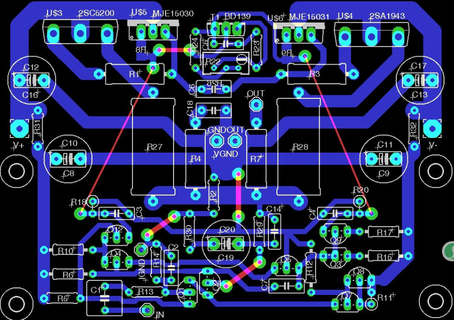
Case Study: Class AB Amplifier PCB Layout
Examining a typical 50W Class AB amplifier design:
- Input Stage:
- Ultra-short traces from RCA inputs to first transistor
- Guard ring around high-impedance base connections
- Separate ground return for input circuitry
- Driver Stage:
- Matched length traces to push-pull transistors
- Local decoupling capacitors within 5mm of each active device
- Output Stage:
- 3mm wide traces for collector connections
- Thermal vias under power transistors
- Symmetrical layout for push-pull pairs
- Power Supply:
- Star-point grounding near main filter capacitors
- Separate charging and discharging capacitor loops
- Twisted pair wiring for transformer secondaries
Tools for Precision PCB Design
Modern EDA (Electronic Design Automation) tools facilitate precision wiring:
- Advanced CAD Features:
- Length matching tools
- Differential pair routers
- 3D visualization for mechanical verification
- Analysis Tools:
- Signal integrity simulation
- Thermal modeling
- EMI prediction
- Manufacturing Integration:
- DFM (Design for Manufacturing) checks
- Automated generation of fabrication files
- Component sourcing integration
Future Trends in Amplifier PCB Design
Emerging technologies impacting precision wiring:
- High-Density Interconnect (HDI): Allows finer traces and closer spacing
- Embedded Components: Passives integrated within PCB layers
- Advanced Materials: High-frequency laminates for ultra-low distortion
- AI-Assisted Layout: Machine learning algorithms suggesting optimal routing
Conclusion
Precision wiring in amplifier PCB design is both an art and a science, requiring careful consideration of electrical, thermal, and mechanical factors. By adhering to fundamental layout principles while employing advanced techniques where needed, designers can create amplifier circuits that deliver the full potential of their schematic designs. The difference between a good amplifier and a great one often lies in the quality of its PCB implementation, where attention to precise wiring details pays dividends in performance, reliability, and sound quality.
As amplifier technologies continue to evolve with Class D, GaN, and other advanced topologies, the principles of precision wiring remain constant—clean signal paths, solid grounding, and thoughtful component placement will always be essential to achieving optimal audio performance. By mastering these techniques and applying them systematically, PCB designers can ensure their amplifier designs perform as intended, delivering clean, powerful audio reproduction with minimal distortion or noise.