Principles and Techniques for Partitioning Design in Mixed-Signal PCBs
Introduction
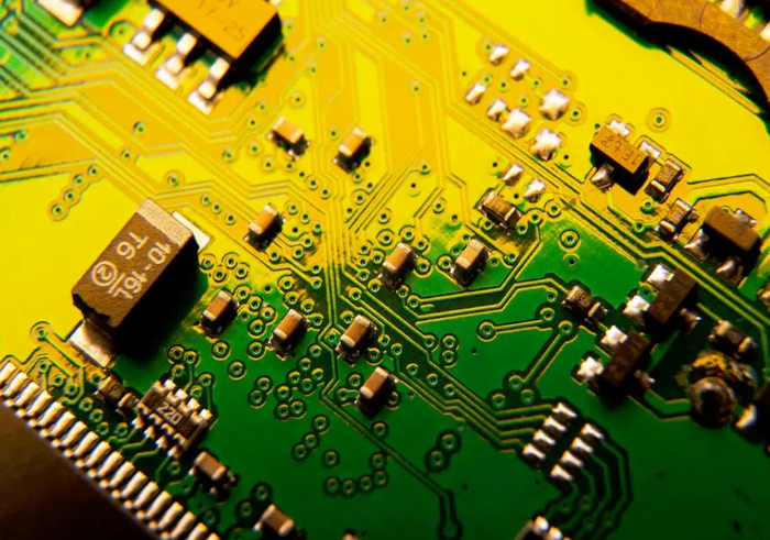
Mixed-signal printed circuit boards (PCBs) that combine both analog and digital circuitry present unique design challenges. Proper partitioning of these mixed-signal boards is critical for maintaining signal integrity, minimizing electromagnetic interference (EMI), and ensuring optimal performance of both analog and digital subsystems. This article explores the fundamental principles of mixed-signal PCB partitioning and provides practical techniques for implementing effective partitioning strategies.
Fundamental Principles of Mixed-Signal PCB Partitioning
1. Separation of Analog and Digital Grounds
The most fundamental principle in mixed-signal PCB design is the proper separation and management of analog and digital ground planes. While these grounds must eventually connect at a single point (typically near the power supply), keeping them separate throughout most of the board prevents digital noise from coupling into sensitive analog circuits.
Key considerations:
- Maintain physical separation between analog and digital ground regions
- Implement a single-point connection (star ground) between the two ground systems
- Ensure low-impedance return paths for all signals
2. Power Domain Isolation
Different power domains should be established for analog and digital sections, with appropriate filtering between them:
- Use separate voltage regulators for analog and digital supplies
- Implement π-filters or ferrite beads at power entry points to each section
- Consider using isolated power supplies for particularly sensitive analog circuits
3. Signal Routing Discipline
Maintain strict routing discipline based on signal type:
- Keep high-speed digital traces away from analog signal paths
- Route sensitive analog signals first, with shortest possible paths
- Avoid crossing analog and digital traces on adjacent layers
- Implement guard traces around critical analog signals
4. Physical Partitioning
The board should be physically divided into distinct analog and digital sections:
- Place all analog components in one area of the board
- Group digital components together in a separate area
- Position mixed-signal devices (ADCs, DACs) at the boundary between sections
5. Component Placement Strategy
Thoughtful component placement supports effective partitioning:
- Position components according to their signal flow through the system
- Place high-speed digital components away from analog inputs
- Locate clock generators and oscillators centrally to minimize trace lengths
Practical Partitioning Techniques
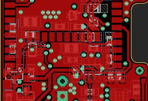
1. Ground Plane Segmentation
Proper ground plane design is crucial for mixed-signal boards:
- Split the ground plane into analog and digital sections
- Connect the planes at a single point near the power supply
- Maintain continuous ground planes under critical analog components
- Avoid slots or splits that could create antenna structures
2. Power Plane Organization
Implement power planes that support the partitioning strategy:
- Use separate power planes for analog and digital supplies
- Consider split power planes for different voltage levels
- Implement proper decoupling for each power domain
3. Layer Stackup Design
Optimize the layer stackup to support partitioning:
- Dedicate adjacent layers to ground planes for shielding
- Route sensitive analog signals between ground planes
- Place digital signal layers away from analog sections
- Use buried layers for critical routing when possible
4. Signal Isolation Techniques
Implement various isolation methods to prevent coupling:
- Use guard rings around sensitive analog nodes
- Implement moats (physical gaps) between analog and digital sections
- Add shielding cans over particularly sensitive components
- Utilize differential signaling for noise immunity
5. Routing Best Practices
Follow specific routing guidelines for mixed-signal boards:
- Maintain adequate spacing between analog and digital traces
- Avoid running digital traces over analog ground areas (and vice versa)
- Implement proper termination for high-speed digital signals
- Use curved traces rather than right angles to minimize reflections
6. Mixed-Signal Component Handling
Special considerations for components that bridge analog and digital domains:
- Place ADCs/DACs at the boundary between analog and digital sections
- Use separate power pins for analog and digital portions of mixed ICs
- Implement proper bypassing for all power pins
- Follow manufacturer recommendations for layout and grounding
7. Clock Distribution Management
Careful clock routing is essential:
- Keep clock traces as short as possible
- Avoid routing clock signals near analog inputs
- Use low-jitter clock sources for sampling circuits
- Consider clock buffer ICs for distributing multiple clocks
8. Partition Verification Techniques
Methods to verify partitioning effectiveness:
- Perform continuity checks to ensure proper ground separation
- Use network analyzers to check for unintended coupling
- Implement frequency-domain analysis to identify noise issues
- Conduct time-domain analysis to verify signal integrity
Advanced Partitioning Strategies
1. Digital Noise Containment
Techniques to contain digital switching noise:
- Implement spread-spectrum clocking for digital circuits
- Use slew rate control for digital outputs when possible
- Group noisy digital components together
- Add local shielding for particularly noisy components
2. Analog Section Protection
Enhanced protection for sensitive analog circuits:
- Implement Faraday cages for critical analog components
- Use low-noise power supplies with excellent regulation
- Consider separate analog ground planes for different subsystems
- Implement feedthrough filters for signals entering analog sections
3. Board Edge Considerations
Special attention to board edges and connectors:
- Provide adequate grounding for board-to-board connectors
- Implement proper ESD protection at I/O boundaries
- Consider separate analog and digital connectors when possible
- Use filtered connectors for analog I/O when appropriate
Common Partitioning Mistakes to Avoid
1. Improper Grounding Practices
- Creating multiple connection points between analog and digital grounds
- Using ground plane splits that create slot antennas
- Failing to provide adequate return paths for high-speed signals
2. Power Supply Errors
- Sharing regulators between analog and digital circuits
- Inadequate decoupling for either domain
- Poor power distribution network design
3. Signal Routing Issues
- Running digital traces through analog sections (or vice versa)
- Failing to maintain proper spacing between different signal types
- Neglecting to consider return current paths when routing
4. Component Placement Problems
- Placing noisy digital components near sensitive analog inputs
- Poor arrangement of mixed-signal components
- Inadequate spacing between components of different types
Case Studies and Practical Examples
1. High-Resolution ADC Implementation
Examine the partitioning requirements for a 24-bit ADC system:
- Extreme isolation requirements for low-level analog signals
- Special grounding considerations for reference voltages
- Power supply filtering needs for optimal performance
- Clock distribution challenges in high-resolution systems
2. RF/Digital Mixed-Signal Board
Partitioning challenges in boards combining RF and digital circuits:
- Special shielding requirements for RF sections
- Grounding considerations for RF circuits
- Power supply isolation techniques
- Interference mitigation strategies
3. Audio Processing System
Partitioning approaches for professional audio equipment:
- Handling very low-level microphone inputs
- Managing high-current amplifier outputs
- Dealing with multiple ground domains
- Implementing star grounding effectively
Future Trends in Mixed-Signal Partitioning
1. 3D Packaging Technologies
How emerging 3D IC technologies may affect partitioning:
- Potential for better isolation between analog and digital sections
- Challenges in thermal management
- New approaches to interconnects between domains
2. Advanced Materials
Impact of new PCB materials on partitioning strategies:
- High-frequency laminates with better isolation properties
- Embedded passive components for improved filtering
- Flexible substrates enabling novel partitioning approaches
3. Automated Partitioning Tools
Development of EDA tools for mixed-signal partitioning:
- AI-assisted placement and routing
- Automated signal integrity analysis
- Simulation-driven partitioning optimization
Conclusion
Effective partitioning is the cornerstone of successful mixed-signal PCB design. By adhering to fundamental principles of ground separation, power domain isolation, and careful signal routing while implementing practical partitioning techniques, designers can create mixed-signal boards that deliver optimal performance for both analog and digital subsystems. As mixed-signal systems continue to increase in complexity, with higher speeds and greater integration, the importance of proper partitioning only grows. Mastering these partitioning principles and techniques enables designers to meet the ever-increasing challenges of modern mixed-signal PCB design.
The key to success lies in understanding the specific requirements of each design, carefully planning the board architecture before layout begins, and verifying the implementation through appropriate analysis and testing. With proper partitioning, mixed-signal designs can achieve their full performance potential while avoiding the pitfalls of noise coupling and interference that plague poorly partitioned boards.