Printed Circuit Assembly Techniques for Enhanced Reliability
Key Takeaways
Effective PCB assembly relies on precision across multiple stages, from soldering optimization to strategic component placement. Modern PCBA processes prioritize thermal management and material durability, particularly for electronics operating in harsh environments. Key innovations include advanced reflow soldering profiles to minimize voids and automated optical inspection (AOI) systems to verify alignment accuracy.
Critical to reliability is the integration of thermal cycling tests, which simulate extreme temperature fluctuations to identify potential failure points. Pairing this with stress analysis techniques—such as finite element modeling—ensures boards withstand mechanical and environmental pressures. Material selection plays a pivotal role, with high-Tg substrates and halogen-free laminates increasingly adopted for enhanced thermal stability.
Emerging methods like 3D solder paste inspection (SPI) and adaptive pick-and-place algorithms further refine assembly consistency. By balancing design-for-manufacturability (DFM) principles with rigorous testing protocols, manufacturers achieve durable circuit boards capable of meeting stringent industry demands. These advancements underscore the importance of harmonizing precision engineering with robust validation frameworks in PCB assembly workflows.
Optimizing Soldering in PCB Assembly
Effective soldering forms the backbone of reliable PCB assembly processes, directly influencing electrical connectivity and mechanical stability. Modern PCBA workflows prioritize techniques like reflow soldering and selective soldering to balance precision with scalability. For instance, reflow soldering employs controlled temperature profiles to melt solder paste uniformly, minimizing voids or cold joints.
Tip: Always validate solder paste viscosity and stencil alignment before reflow to prevent bridging or insufficient solder deposition.
Critical parameters in soldering optimization include:
| Factor | Ideal Range | Impact on Reliability |
|---|---|---|
| Peak Temperature | 230–250°C | Prevents component thermal stress |
| Cooling Rate | 1–3°C/sec | Reduces intermetallic compound brittleness |
| Solder Alloy | SAC305 (Sn96.5/Ag3/Cu0.5) | Enhances thermal fatigue resistance |
In harsh environments, lead-free alloys paired with automated optical inspection (AOI) systems ensure joint integrity under thermal cycling. Additionally, nitrogen-assisted soldering reduces oxidation, particularly for fine-pitch components. For mixed-technology boards combining SMD and through-hole parts, sequential soldering methods mitigate heat-related warping.
Advanced PCB assembly lines now integrate real-time thermal profiling, adjusting parameters dynamically based on component density and substrate material. This adaptability is crucial for aerospace or automotive applications, where solder joint failures can lead to catastrophic system breakdowns. By aligning process controls with material science advancements, manufacturers achieve sub-10µm placement accuracy while maintaining repeatability across high-volume production runs.
PCB Component Placement Strategies
Effective PCB assembly relies on strategic component placement to balance performance, manufacturability, and long-term reliability. Thermal management begins with positioning heat-generating components—such as power regulators or processors—away from temperature-sensitive parts like sensors or electrolytic capacitors. This minimizes thermal interference and reduces the risk of premature failure in PCBA systems operating under load.
Signal integrity demands careful routing of high-speed traces, ensuring minimal cross-talk by spacing analog and digital sections appropriately. For example, placing clock generators closer to their target ICs shortens trace lengths, mitigating timing errors. Mechanical stability is equally critical: heavier components, such as transformers or connectors, should be anchored near mounting points to withstand vibration or shock in harsh environments.
Automated PCB assembly workflows leverage design-for-manufacturing (DFM) guidelines to optimize pick-and-place efficiency. Aligning components uniformly along X/Y axes reduces machine repositioning, accelerating production while maintaining placement accuracy below 50µm. Additionally, grouping surface-mount devices (SMDs) on one side simplifies reflow soldering, whereas through-hole parts may require strategic spacing for manual rework access.
Finally, testability considerations guide placement of test points and debug headers. Positioning these near critical nodes—like power inputs or communication buses—facilitates in-circuit testing (ICT) and fault isolation during quality assurance. By integrating these principles, engineers ensure PCBA designs meet both functional and reliability benchmarks across their lifecycle.
Harsh Environment Material Selection
Selecting appropriate materials for PCB assembly in harsh environments requires balancing thermal stability, chemical resistance, and mechanical durability. High-reliability PCBA designs often utilize substrates like polyimide or ceramic-filled laminates, which outperform standard FR-4 in extreme temperatures. For instance, polyimide’s glass transition temperature (Tg) exceeding 260°C prevents delamination during rapid thermal cycling, a critical factor in aerospace or automotive applications.
Conformal coatings play an equally vital role, with silicone-based or parylene layers providing robust protection against moisture, dust, and corrosive agents. Engineers often specify lead-free solder alloys with higher silver content to mitigate joint fatigue under vibration or shock—common in industrial automation systems. Additionally, selecting components rated for extended temperature ranges (-55°C to 150°C) ensures consistent performance in subzero or high-heat conditions.
Material compatibility with PCB assembly processes is equally crucial. For example, low-voiding underfills enhance structural integrity in PCBA exposed to mechanical stress, while halogen-free laminates meet stringent environmental regulations. By aligning material properties with operational demands, manufacturers achieve predictable longevity even in settings prone to thermal shocks, humidity fluctuations, or chemical exposure. This systematic approach forms the foundation for reliability in mission-critical electronics.
Thermal Cycling Test Techniques
Effective thermal cycling tests are critical for evaluating long-term reliability in PCB assembly processes, particularly for PCBA destined for harsh environments. These tests simulate extreme temperature fluctuations—from subzero conditions to elevated heat—to replicate real-world operational stresses. By subjecting assemblies to repeated thermal expansion and contraction, engineers can identify weaknesses in solder joints, substrate adhesion, and component interfaces.
Modern thermal cycling protocols combine empirical data with computational modeling to optimize test parameters, such as temperature ramp rates and dwell times. For example, accelerated life testing (ALT) exposes PCBA to rapid temperature swings, revealing failure modes like solder joint cracking or delamination. Advanced systems incorporate real-time monitoring of electrical continuity during cycles, enabling precise detection of intermittent failures.
A key consideration is aligning test conditions with the end-use environment. Automotive or aerospace applications, for instance, demand stricter thermal profiles than consumer electronics. Material selection plays a pivotal role here—high-CTE (coefficient of thermal expansion) mismatches between components and substrates often accelerate fatigue. Through controlled exposure to thermal stress, manufacturers validate design choices, refine PCB assembly workflows, and ensure compliance with industry-specific durability standards.
Stress Analysis for PCB Reliability
Effective PCB assembly processes must account for mechanical and thermal stresses that threaten long-term reliability, particularly in harsh operating environments. Stress analysis techniques, such as finite element analysis (FEA), simulate how forces like vibration, thermal expansion, or mechanical shock propagate through a PCBA during its lifecycle. By mapping stress concentrations at solder joints, component interfaces, or substrate layers, engineers can identify weak points prone to fatigue or fracture. For instance, thermal cycling tests often reveal differential expansion rates between copper traces and FR-4 substrates, necessitating adjustments in material selection or component placement to mitigate delamination risks.
Advanced PCB assembly workflows integrate real-world stress data to refine designs—optimizing pad geometries, reinforcing high-stress zones with additional vias, or selecting conformal coatings with matched coefficients of thermal expansion. Accelerated life testing further validates these improvements by replicating years of environmental exposure in compressed timelines. This analytical approach ensures that PCBA designs not only meet initial performance criteria but also endure cyclical stresses without compromising electrical integrity. By aligning simulation results with empirical testing, manufacturers achieve a balance between precision and durability, critical for applications ranging from aerospace systems to industrial automation.
Advanced PCB Assembly Methods
Modern PCB assembly processes leverage cutting-edge technologies to address evolving demands for precision and resilience. Central to PCBA advancements is the integration of automated optical inspection (AOI) systems, which validate solder joint quality and component alignment at micron-level tolerances. These systems work in tandem with 3D solder paste inspection (SPI) tools to preempt defects before reflow soldering, reducing post-production rework by up to 40%.
Another critical advancement lies in mixed-technology assembly, combining surface-mount (SMT) and through-hole components to optimize performance in complex layouts. For high-reliability applications, vacuum-assisted placement ensures secure mounting of micro-BGA and QFN packages, mitigating voids in underfill materials. Additionally, sequential lamination techniques enable multilayer boards to withstand thermal expansion mismatches in harsh environments.
Emerging PCBA workflows now incorporate predictive process control, using machine learning algorithms to analyze historical production data. This approach fine-tunes parameters like reflow profiles and nitrogen levels in soldering ovens, enhancing consistency across batches. To further bolster reliability, in-situ thermal profiling monitors heat distribution during assembly, preventing latent stresses that could compromise long-term functionality.
By harmonizing these innovations, manufacturers achieve tighter integration between design intent and PCB assembly execution, laying the foundation for electronics that excel under extreme operational conditions.
Enhancing Circuit Board Durability
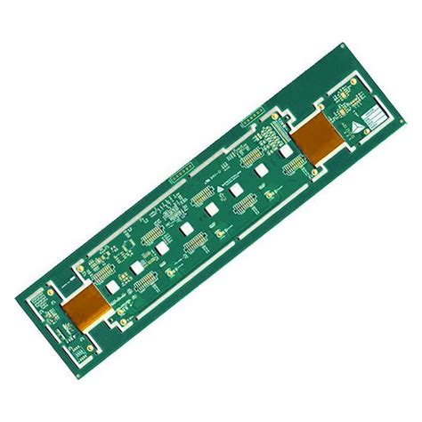
Improving the longevity of PCB assembly requires a systematic approach to address environmental stressors and operational demands. A critical factor lies in selecting high-performance substrates with low coefficient of thermal expansion (CTE), which minimizes warping during thermal cycling tests. For PCBA destined for harsh environments, materials like polyimide or ceramic-filled laminates offer superior resistance to moisture, chemicals, and temperature extremes.
Equally vital is optimizing mechanical reinforcement through strategic component placement and underfill applications. Staggering heat-sensitive components away from high-power devices reduces localized stress, while epoxy underfills enhance solder joint integrity under vibration. Advanced stress analysis techniques, such as finite element analysis (FEA), simulate mechanical and thermal loads to identify weak points in the design phase.
To further validate durability, thermal cycling tests should replicate real-world conditions, including rapid temperature fluctuations and prolonged exposure to humidity. Pairing these tests with accelerated life testing (ALT) ensures that PCB assembly meets reliability benchmarks before deployment. By integrating robust materials, precision PCBA processes, and rigorous validation protocols, manufacturers can significantly extend the operational lifespan of electronic systems in demanding applications.
Precision Techniques in PCB Manufacturing
Achieving high reliability in PCB assembly requires meticulous attention to precision at every stage of manufacturing. Modern PCBA processes integrate advanced technologies such as automated optical inspection (AOI) and laser-aligned stencil printing to ensure micrometer-level accuracy in solder paste deposition. These methods minimize defects like bridging or insufficient solder joints, which are critical for maintaining signal integrity in high-frequency applications.
A key focus lies in optimizing component placement through vision-guided robotic systems capable of positioning microscale components (e.g., 0201 resistors or QFN packages) with ±25-micron precision. This is particularly vital for dense layouts found in IoT devices or aerospace electronics, where spatial constraints demand flawless alignment. Additionally, controlled atmosphere reflow ovens mitigate oxidation during soldering, enhancing joint strength and thermal resilience.
To further refine precision, manufacturers employ inline metrology tools for real-time dimensional verification, ensuring compliance with design tolerances. This integration of measurement and correction loops within PCB assembly workflows reduces rework rates by up to 40%, directly contributing to long-term reliability. Such techniques, when combined with rigorous material selection and process validation, establish a foundation for PCBA solutions that thrive in mission-critical environments.
Conclusion
The evolution of PCB assembly techniques underscores the critical balance between precision engineering and rigorous validation. Modern PCBA processes leverage advancements in automated soldering and component placement to minimize human error, ensuring consistent performance even in harsh environments. By integrating thermal cycling tests and stress analysis, manufacturers can simulate real-world operational challenges, identifying potential failure points before deployment.
Material selection remains pivotal—high-grade substrates, conformal coatings, and lead-free solder alloys enhance durability without compromising conductivity. These innovations, combined with data-driven process optimization, enable PCB assembly workflows to meet escalating demands for reliability in aerospace, automotive, and industrial applications.
Ultimately, the synergy between advanced manufacturing technologies and stringent quality assurance protocols defines the future of PCBA. As electronic systems grow more complex, prioritizing failure mode analysis and preventive testing will remain indispensable for delivering robust, long-lasting solutions. This holistic approach not only safeguards functionality but also aligns with evolving industry standards for sustainability and resilience.
Frequently Asked Questions
What distinguishes high-reliability PCB assembly from standard processes?
PCB assembly (PCBA) for demanding environments prioritizes soldering precision, thermal-resistant materials, and rigorous testing. Advanced techniques like automated optical inspection (AOI) and X-ray verification ensure micro-level accuracy, while thermal cycling tests validate performance under extreme temperature fluctuations.
How does component placement affect long-term reliability in harsh conditions?
Strategic component placement minimizes mechanical stress and heat concentration. Critical components are positioned away from high-vibration zones, and surface-mount technology (SMT) optimizes solder joint integrity. This approach, combined with stress analysis simulations, reduces failure risks in corrosive or high-humidity environments.
Which materials enhance durability in extreme-environment PCBA?
High-Tg FR-4 substrates, lead-free solders, and conformal coatings provide resistance to thermal expansion and chemical exposure. For aerospace or automotive applications, ceramic-filled laminates and silicon-based encapsulants further improve stability during thermal cycling tests.
Why are thermal cycling tests mandatory for industrial-grade assemblies?
These tests replicate real-world temperature swings to identify weak points in solder joints or materials. By exposing PCBA prototypes to controlled cycles, engineers validate thermal management strategies and ensure compliance with MIL-STD-883 or IPC-9701 standards.
Can stress analysis prevent field failures in PCB assemblies?
Yes. Finite element analysis (FEA) models mechanical and thermal stresses, guiding design adjustments before production. This proactive approach identifies potential cracks or delamination, aligning with reliability-focused PCBA workflows.
Explore Customized PCB Assembly Solutions
For tailored PCB assembly services optimized for harsh environments, please click here to consult our engineering team.


