Printed Circuit Boards: Design, Fabrication, and Assembly
Introduction
Printed Circuit Boards (PCBs) are an integral part of modern electronic devices. They not only provide mechanical support for electronic components, but also connect components through conductive paths to ensure the smooth flow of current. With the continuous advancement of technology, the design, manufacturing, and assembly processes of PCBs are also evolving. This article will explore the design, manufacturing, and assembly processes of PCBs in depth, analyze their importance in electronic products, and analyze their future development trends.
1.PCB Design
1.1 Design Basics
PCB design is a complex process involving multiple steps and considerations. Designers first need to understand the functional requirements of the circuit and perform preliminary circuit design based on these requirements. Commonly used design software includes Altium Designer, Eagle, KiCAD, etc. These tools can help designers create circuit schematics and PCB layouts.
1.2 Circuit Schematics
The circuit schematic is the first step in PCB design. Designers need to draw the various components of the circuit and their connections in the software. This stage requires consideration of component selection, pin configuration, and power and ground layout. After the schematic is completed, the designer needs to perform circuit simulation to ensure that the circuit can operate normally in actual work.
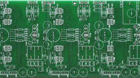
1.3 PCB layout
After completing the circuit schematic, the designer converts it into a PCB layout. The layout process includes the following key steps:
Component placement: Arrange the position of components according to the circuit function and signal flow to minimize signal interference and delay.
Wiring: Designers need to draw electrical connection lines on the PCB to ensure signal integrity and effective current transmission.
Layer selection: Depending on the complexity of the circuit, the designer needs to decide the number of layers of the PCB. Single-sided, double-sided and multi-layer boards each have their own applicable scenarios.
Design rule check (DRC): Ensure that the layout meets manufacturing standards and avoids problems such as short circuits and open circuits.
1.4 Design verification
After the design is completed, verification must be performed. Design verification includes electrical rule checking (ERC) and signal integrity analysis. Designers need to ensure that all electrical connections are correct and the transmission of signals on the PCB is not interfered with.
2.PCB Manufacturing
2.1 Overview of Manufacturing Process
The manufacturing process of PCB usually includes the following steps:
Material preparation: Select suitable substrate (such as FR-4, CEM-1, etc.) and copper foil.
Graphic transfer: Transfer the circuit pattern to the substrate through photolithography.
Etching: Remove excess copper foil to form the circuit pattern.
Punching: Punch holes on the PCB according to design requirements to facilitate component installation.
Electroplating: Plate a layer of metal in the hole and on the surface to improve conductivity.
Surface treatment: Treat the surface of the PCB to improve welding performance and corrosion resistance.
Cutting and testing: Cut the PCB into the required size and perform electrical testing.
2.2 Material selection
The material selection of PCB is crucial to its performance and reliability. Common PCB materials include:
FR-4: A commonly used glass fiber reinforced epoxy resin material with good insulation and mechanical strength.
CEM-1: A low-cost material suitable for simple single-sided PCBs.
Aluminum substrate: used for high-power applications, with good heat dissipation performance.
2.3 Advanced manufacturing technology
With the development of science and technology, PCB manufacturing technology is also constantly improving. For example, laser drilling technology can achieve higher-precision hole processing, while high-density interconnection (HDI) technology can achieve more circuit connections in a smaller space.
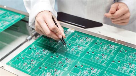
3. PCB assembly
3.1 Assembly process
The assembly process of PCB usually includes the following steps:
Printing solder paste: Apply solder paste evenly to the soldering points of the PCB.
SMD: Place surface mount components (SMD) on the solder paste.
Reflow soldering: Put the PCB into the reflow oven and melt the solder paste by heating to form a strong connection.
Plug-in components: For components that need to be inserted into the hole, plug-in soldering is performed.
Cleaning: Remove impurities generated during the soldering process.
Testing: Perform functional tests on the assembled PCB to ensure that it works properly.
3.2 Assembly technology
In PCB assembly, commonly used technologies include:
Surface mount technology (SMT): suitable for the assembly of high-density components and can improve production efficiency.
Through-hole technology (THT): suitable for the assembly of larger components, usually used in applications that need to withstand greater mechanical stress.
3.3 Automated assembly
With the advancement of Industry 4.0, the degree of automation of PCB assembly is getting higher and higher. Automated equipment can improve production efficiency and reduce the rate of human error. In addition, the application of intelligent manufacturing technology makes data collection and analysis in the production process easier, thereby achieving more efficient production management.
4. Application and development trend of PCB
4.1 Application field
PCB is widely used in various fields, including:
Consumer electronics: such as mobile phones, tablets, TVs, etc.
Industrial control: such as automation equipment, sensors, etc.
Medical equipment: such as monitoring instruments, diagnostic equipment, etc.
Automotive electronics: such as in-vehicle navigation, power system control, etc.
4.2 Future development trend
With the continuous advancement of science and technology, the PCB industry is also developing. Future trends include:
More miniaturization and lightweight: As electronic products develop towards miniaturization and lightweight, the design and manufacture of PCBs will face new challenges.
High-frequency and high-speed applications: With the development of 5G technology, the demand for high-frequency and high-speed PCBs will continue to increase.
Application of environmentally friendly materials: As environmental awareness increases, PCB manufacturing will gradually transform to environmentally friendly materials.
Intelligence and automation: Intelligent manufacturing will become the main trend in PCB production, improving production efficiency and product quality.
Conclusion
As the core component of modern electronic devices, the design, manufacturing and assembly process of printed circuit boards is crucial. With the continuous advancement of science and technology, the PCB industry is also constantly developing and facing new challenges and opportunities. Understanding the various aspects of PCBs will not only help improve the performance and reliability of electronic products, but also provide a foundation for future innovations. I hope this article can provide readers with a comprehensive understanding of PCB design, manufacturing and assembly, and stimulate interest in this field.


