Process of pcb manufacturing
Introduction To PCB Manufacturing: From Design To Production
Printed Circuit Boards (PCBs) are the backbone of modern electronic devices, providing the necessary platform for electronic components to communicate and function. The process of PCB manufacturing is intricate and involves several stages, each critical to ensuring the final product meets the required specifications and performance standards. This article delves into the journey of PCB manufacturing, from the initial design phase to the final production stage.
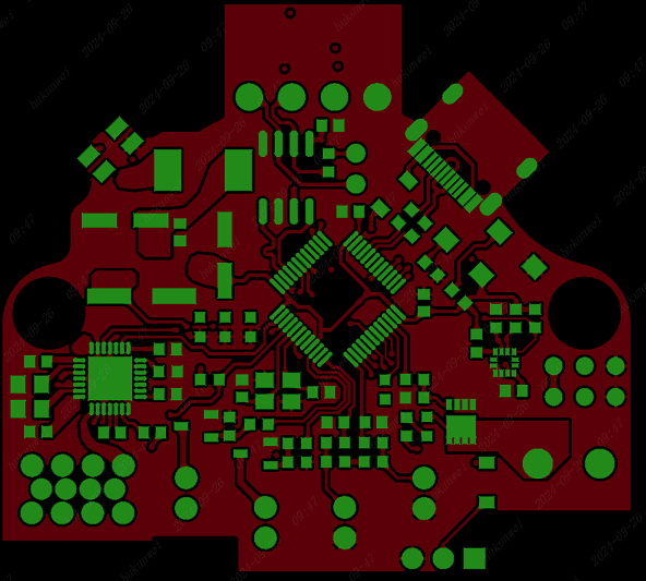
The process begins with the design phase, where engineers and designers use specialized software to create a detailed blueprint of the PCB.
This blueprint includes the layout of the circuit, the placement of components, and the routing of electrical connections. The design must adhere to specific guidelines and standards to ensure functionality and manufacturability. Once the design is finalized, it is converted into a format that can be used by the manufacturing equipment, typically Gerber files.
Following the design phase, the next step is the creation of the PCB substrate, which serves as the foundation for the circuit.
.The substrate is usually made of a non-conductive material, such as fiberglass or epoxy resin, which provides mechanical support and electrical insulation. A thin layer of copper is then laminated onto the substrate to form the conductive pathways. This copper layer is essential for creating the electrical connections between components.
The subsequent stage involves the application of a photoresist, a light-sensitive material, onto the copper-clad substrate.
The photoresist is then exposed to ultraviolet (UV) light through a photomask, which contains the pattern of the circuit. The areas of the photoresist exposed to UV light harden, while the unexposed areas remain soft and can be washed away. This process creates a precise pattern of the circuit on the copper layer.
Once the photoresist pattern is established, the next step is etching.
During etching, a chemical solution is used to remove the unprotected copper, leaving behind only the desired circuit pattern. This step is crucial, as it defines the electrical pathways that will connect the various components on the PCB. After etching, the remaining photoresist is stripped away, revealing the final copper circuit.
The process then moves to drilling, where holes are created in the PCB to accommodate component leads and vias, which are used to connect different layers of the board.
Precision drilling machines are employed to ensure accuracy and consistency in hole placement and size. These holes are then plated with copper to establish electrical connections between layers.
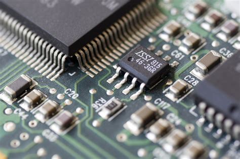
Following drilling and plating, the PCB undergoes a solder mask application.
The solder mask is a protective layer that covers the copper traces, preventing short circuits and oxidation. It also helps to define the areas where solder will be applied during component assembly. The solder mask is typically applied using a screen-printing process and then cured using UV light.
The final stages of PCB manufacturing involve the application of a silkscreen layer,
which adds labels and markings to the board, and the surface finish, which protects the exposed copper and enhances solderability. Common surface finishes include HASL (Hot Air Solder Leveling), ENIG (Electroless Nickel Immersion Gold), and OSP (Organic Solderability Preservative).
In conclusion, the process of PCB manufacturing is a complex and multi-faceted journey that transforms a conceptual design into a tangible product. Each stage, from design to production, requires precision and attention to detail to ensure the final PCB meets the desired specifications and performance criteria. Understanding this process is essential for anyone involved in the electronics industry, as it underscores the intricate craftsmanship behind the technology that powers our modern world.

Key Steps In PCB Fabrication: A Detailed Guide
Printed Circuit Boards (PCBs) are the backbone of modern electronic devices, providing the necessary support and connectivity for various electronic components. The process of PCB manufacturing is intricate and involves several key steps, each crucial to ensuring the final product’s functionality and reliability. Understanding these steps provides insight into the complexity and precision required in PCB fabrication.
The journey begins with the design phase, where engineers use specialized software to create a detailed blueprint of the PCB.
This design includes the layout of the circuit, the placement of components, and the routing of electrical connections. Once the design is finalized, it is converted into a format suitable for manufacturing, typically Gerber files, which contain all the necessary information for each layer of the PCB.
Following the design phase, the next step is the creation of the PCB substrate, usually made from a material like fiberglass or epoxy resin.
This substrate serves as the foundation of the PCB. A thin layer of copper is then laminated onto the substrate, forming the base for the circuit’s conductive pathways. The copper layer is essential for creating the electrical connections between components.
The subsequent step involves transferring the circuit design onto the copper-clad substrate.
This is achieved through a process called photolithography. A photosensitive film, known as a photoresist, is applied to the copper surface. The Gerber files are used to create a photomask, which is then placed over the photoresist-coated substrate. When exposed to ultraviolet light, the photoresist hardens in the areas exposed through the photomask, while the unexposed areas remain soft and can be washed away. This leaves a precise pattern of the circuit design on the copper layer.
Etching follows photolithography, where the exposed copper areas are removed using a chemical solution, typically ferric chloride or ammonium persulfate.
This process leaves behind the desired copper traces that form the circuit. After etching, the remaining photoresist is stripped away, revealing the clean copper pathways.
Drilling is the next critical step, where holes are drilled into the PCB to accommodate component leads and vias, which are conductive pathways that connect different layers of the PCB. Precision is paramount in this step, as any misalignment can lead to connectivity issues. Advanced drilling machines, often guided by computer numerical control (CNC), ensure accuracy and consistency.
Once drilling is complete, the PCB undergoes a plating process to coat the drilled holes with a thin layer of copper, ensuring electrical connectivity between layers.
This is followed by the application of a solder mask, a protective layer that insulates the copper traces and prevents solder bridges during component assembly. The solder mask is typically green but can come in various colors.
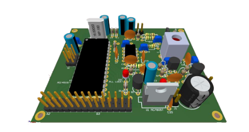
The final steps involve the application of a silkscreen layer, which adds labels and markings to the PCB, aiding in component placement and identification.
The PCB then undergoes a series of inspections and tests to verify its integrity and functionality. These tests include electrical testing to check for continuity and shorts, as well as visual inspections to ensure there are no defects.
In conclusion, PCB manufacturing is a meticulous process that requires precision and attention to detail at every stage. From design and substrate preparation to etching, drilling, and final testing, each step is vital to producing a reliable and functional PCB. Understanding these key steps highlights the complexity and expertise involved in bringing modern electronic devices to life.
Quality Control In PCB Manufacturing: Ensuring Reliability
Quality control in PCB manufacturing is a critical aspect that ensures the reliability and functionality of the final product. The process begins with the design phase, where engineers meticulously plan the layout and specifications of the printed circuit board. This initial stage is crucial, as any errors in the design can lead to significant issues down the line. To mitigate this risk, design verification tools are employed to simulate and test the PCB layout before it moves to the manufacturing phase.
Once the design is verified, the next step involves the procurement of raw materials.
High-quality materials are essential for producing reliable PCBs, and suppliers are carefully vetted to ensure they meet stringent quality standards. Upon receiving the materials, they undergo rigorous inspection to confirm their compliance with the required specifications. This step is vital, as substandard materials can compromise the integrity of the entire manufacturing process.
Following material inspection, the manufacturing process begins with the creation of the PCB layers.
This involves several steps, including etching, drilling, and plating. Each of these steps is closely monitored to ensure precision and accuracy. For instance, during the etching process, the unwanted copper is removed to create the desired circuit patterns. Any deviation from the specified patterns can lead to circuit failures, making it imperative to maintain strict control over this process.
As the PCB layers are formed, they are subjected to various tests to verify their quality.
One such test is the Automated Optical Inspection (AOI), which uses high-resolution cameras to detect any defects in the PCB layers. This non-contact method allows for rapid and accurate identification of issues, ensuring that only flawless layers proceed to the next stage.
Subsequently, the layers are laminated together to form a multi-layer PCB.
This lamination process requires precise control of temperature and pressure to ensure a strong bond between the layers. Any inconsistencies in this process can result in delamination, which can severely impact the PCB’s performance. Therefore, continuous monitoring and adjustments are made to maintain optimal conditions.
Once the lamination is complete, the PCBs undergo electrical testing to verify their functionality.
This involves checking for continuity and isolation to ensure that the circuits are correctly formed and there are no short circuits or open circuits. Electrical testing is a crucial step, as it confirms that the PCB will perform as intended in its final application.
In addition to electrical testing, environmental stress tests are conducted to assess the PCB’s durability under various conditions.
These tests simulate extreme temperatures, humidity, and mechanical stress to ensure that the PCB can withstand harsh environments. By subjecting the PCBs to these rigorous tests, manufacturers can identify potential weaknesses and make necessary improvements.
Finally, the PCBs are inspected for any physical defects, such as scratches, misalignments, or soldering issues.
This final inspection ensures that the PCBs meet the highest quality standards before they are shipped to customers. Any defects identified at this stage are rectified or the PCB is discarded to maintain the overall quality of the batch.
In conclusion, quality control in PCB manufacturing is a comprehensive process that encompasses design verification, material inspection, precise manufacturing, and rigorous testing. Each step is meticulously monitored to ensure that the final product is reliable and meets the required specifications. By adhering to these stringent quality control measures, manufacturers can deliver high-quality PCBs that perform reliably in their intended applications.

Innovations In PCB Manufacturing: Trends And Technologies
The process of PCB manufacturing has undergone significant transformations over the years, driven by continuous innovations and the adoption of advanced technologies. These advancements have not only enhanced the efficiency and precision of PCB production but have also opened new avenues for design and application.
One of the most notable trends in PCB manufacturing is the shift towards automation.
Automated processes, such as robotic assembly and automated optical inspection (AOI), have significantly reduced human error and increased production speed. This automation is complemented by the use of sophisticated software tools that enable precise design and simulation, ensuring that the final product meets stringent quality standards.
In addition to automation, the integration of advanced materials has played a crucial role in the evolution of PCB manufacturing.
High-performance substrates, such as polyimide and ceramic-based materials, offer superior thermal and electrical properties compared to traditional FR4 substrates. These materials are particularly beneficial in applications that require high reliability and performance, such as aerospace and medical devices. Furthermore, the development of flexible PCBs has expanded the possibilities for electronic design, allowing for more compact and versatile devices.
Another significant innovation in PCB manufacturing is the adoption of additive manufacturing techniques, commonly known as 3D printing.
This technology enables the creation of complex PCB structures that would be challenging or impossible to achieve with traditional subtractive methods. 3D printing also allows for rapid prototyping, reducing the time and cost associated with developing new PCB designs. As a result, manufacturers can quickly iterate and refine their products, accelerating the overall development cycle.
The trend towards miniaturization has also influenced PCB manufacturing processes.
As electronic devices become smaller and more powerful, the demand for compact and densely packed PCBs has increased. This has led to the development of advanced fabrication techniques, such as laser drilling and microvia technology, which allow for the creation of smaller and more precise features on the PCB. Additionally, the use of high-density interconnect (HDI) technology has enabled the production of multi-layer PCBs with intricate routing and interconnections, further enhancing the performance and functionality of electronic devices.
Environmental considerations have also become a driving force in the evolution of PCB manufacturing.
The industry has made significant strides in adopting eco-friendly practices, such as the use of lead-free solder and the implementation of recycling programs for PCB waste. Moreover, advancements in chemical processes have led to the development of more sustainable and less hazardous materials, reducing the environmental impact of PCB production.
The rise of the Internet of Things (IoT) has further influenced PCB manufacturing trends.
IoT devices often require specialized PCBs that can support wireless communication and low-power operation. This has spurred the development of new design methodologies and manufacturing techniques tailored to the unique requirements of IoT applications. For instance, the use of embedded components and system-in-package (SiP) technology has become more prevalent, enabling the integration of multiple functions into a single, compact PCB.
In conclusion, the process of PCB manufacturing continues to evolve, driven by innovations in automation, materials, additive manufacturing, miniaturization, environmental sustainability, and the demands of emerging technologies like IoT. These advancements have not only improved the efficiency and quality of PCB production but have also expanded the possibilities for electronic design and application. As the industry continues to innovate, we can expect further enhancements in PCB manufacturing processes, paving the way for the next generation of electronic devices.