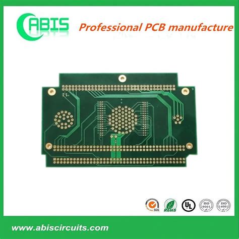
Production skills of optical printed circuit boards
Electronic enthusiasts often make circuit boards by themselves. It is difficult to make high-quality circuit boards using traditional copper-clad boards. This article introduces an optical printed circuit board. The plate making process is time-saving and labor-saving, the process is simple, double-sided wiring can be done, and the quality of the produced circuit boards is very high. Among them, the “Golden Electronics” optical printed circuit boards produced by Taiwanese factories are of very good quality. The following are the specific production steps:
(1) Production of the original manuscript: A. First design the circuit diagram using circuit design software, and then use a laser printer to print out the base map on transparent, semi-transparent or ordinary white paper.
Inkjet printers can barely be used, but the quality is poor, and dot matrix printers cannot be used. B. You can use a photoplotter or photographic film to output the base map, which has the best effect. C. Now there is a kind of thermal transfer paper. You can use a special thermal transfer machine to transfer the image to the thermal transfer paper to obtain the base map.
(2) Cutting: Take the photosensitive board out of the packaging bag, cut off the protective film with a paper cutter, and then cut the circuit board to the required size with a saw or a cutter. To prevent poor adhesion, use a file to smooth the rough edges of the circuit board. Put the remaining photosensitive board back into the bag and store it in a cool and dark place. Be careful not to peel off the protective paper when cutting to prevent scratching or staining the photosensitive surface. The bakelite board can also be cut with a knife to a depth of about 0.2mm on both sides, and then break it.
(3) Exposure: First tear off the protective film to expose the grass green photosensitive film, place the back of the transparent or translucent original on the photosensitive board, and then use transparent glass to press the original and the photosensitive board tightly. The tighter the resolution, the better. The exposure distance and time vary with different lighting. The specific method is described below.
1) Exposure with fluorescent desk lamp: The distance between the glass and the lamp tube is 5CM (±1CM), the standard time for transparent draft is 8 minutes ±2 minutes, and the standard time for translucent draft is 10 minutes. If the width of the board exceeds 10CM, 2 fluorescent lamps are required for average irradiation or partition exposure, and the exposure time is increased by 20%.
2) Exposure with Jin Electronics special exposure machine: The standard time for transparent draft is 60 seconds, and the standard time for translucent draft is 70 seconds.
3) Exposure with sunlight: The standard time is 1.5 minutes in strong sunlight and 3 minutes in weak light.
When making double-sided boards, 2-3 positioning holes must be added to the original, and holes must be drilled on the photoprinting board according to this position, so that the front and back originals are aligned with the holes on the photoprinting board, and fixed with double-sided tape, and then exposed.
The following points must be noted during this process:
1) The exposure process does not need to be operated in a darkroom, as long as it is in a not too bright room or a place where direct sunlight cannot reach.
2) Pay attention to the front and back of the manuscript, that is, stick the back of the manuscript to the photosensitive film surface.
3) The glass must be flat, clean, and pressed tightly against the photosensitive plate. Be careful not to scratch the photosensitive film surface to avoid line breakage. Keep the plate surface and manuscript clean.
4) Do not use incandescent lamps for exposure. Pay special attention not to overexpose, otherwise the image will develop too quickly and the lines will become thinner and disappear.
4.Development:
1) Prepare the developer: Use a plastic basin to mix the developer in proportion (developer: water = 1:2), that is, add 1000 ml of water to 1 package of 50g developer to dilute it into the developer.
2) Development: Put the exposed photosensitive plate film face up into the developer, and gently shake the container or photosensitive plate every few seconds to make the lines clearly appear. That is, the copper foil is clear and there is no green mist rising, then the development is complete. At this time, you need to wait for a while and confirm that the development is 100% complete before washing with water.
3) Washing: The standard development time is about 1 minute. After development, use clean water and blow dry with a blower. The development time varies with the manufacturing date, exposure time, developer concentration, temperature, etc. of the photosensitive plate. That is, the developer concentration of the photosensitive plate increases by 20% every six months since the date of manufacture; if the developer concentration is too thin or underexposed, the development time will be too long and the photosensitive film will remain, so the lines cannot be completely clear; on the contrary, if the developer concentration is too thick or overexposed, the development will be too fast and the lines will be too thin and disappear completely; the suitable temperature is 10-35 degrees, and the higher the temperature, the faster the development speed. 1 pack of developer can develop about 20 10×15CM single-sided photosensitive plates. When washing double-sided plates with water, be careful not to let the bottom of the basin damage the film surface.
During the development process, it is necessary to pay attention to the following:
1) Used and unused developer solutions cannot be mixed together.
2) The developer cannot be mixed with ferric oxide solution, otherwise it will fail.
3) One package of developer can only develop about 20 10×15CM single-sided photosensitive plates.
4) Be careful not to scratch the film surface.
5) The developer can be kept for about one day after development, and then it will decompose by itself without causing environmental pollution.
(5) Film repair: In order to ensure that there is no damage to the film surface, the dried photosensitive plate should be fully inspected. If there is any short circuit, it should be scraped clean with a knife, and the broken wire should be repaired with an oil pen.
(6) Etching: Heat the 1:1 etching solution made of ferric chloride to 50℃-60℃, put the photosensitive plate film face up in it, shake the container gently until the nonlinear part is completely etched away, and then rinse it with water. Use a plastic basin for etching (avoid using a metal basin). The mixing ratio of ferric chloride etching solution is: block ferric chloride: water = 1:2, liquid ferric chloride: water = 1:0.5, and the etching time is about 20-60 minutes. Etching with a gold electronic etching machine takes about 4-5 minutes for a new solution. During the etching process, you need to master the skills and precautions.
Here are a few points for your reference:
1) After the photosensitive plate is placed in the etching solution, take it up and inspect it for about 20 seconds. The copper foil of the nonlinear part should be pink. If it is bright green, it means that the image is insufficient. Wash it with clean water and develop it again, but be careful not to overdo it (reducing the development time appropriately).
2) Be careful not to damage the film surface during etching to prevent the circuit from being broken.
3) Only acidic etching solutions can be used for photosensitive plates, not alkaline etching solutions.
4) The thicker the ferric chloride etching solution, the slower it will be. The thinner it is, the slower it will be.
(7) Film removal: The photosensitive film can be directly welded without removal. If it needs to be removed, alcohol, acetone and other solvents can be used. If it is not removed, high-quality solder must be used; if it needs to be removed, use a cloth dipped in a thicker developer or alcohol to wipe off the remaining film layer. After removing the film layer, the circuit board should be coated with rosin water or PCB board protective agent.