Proper Maintenance Methods for PCB Boards
Introduction
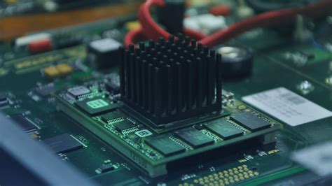
Printed Circuit Boards (PCBs) are the backbone of modern electronic devices, serving as the foundation for electrical connections between components. Proper maintenance of PCBs ensures their longevity, reliability, and optimal performance. Neglecting PCB care can lead to corrosion, electrical failures, and reduced efficiency. This article outlines essential maintenance methods for PCBs, including cleaning, inspection, environmental control, and handling best practices.
1. Regular Cleaning of PCBs
Dust, dirt, and contaminants can accumulate on PCBs over time, leading to short circuits, overheating, and signal interference. Regular cleaning is crucial to prevent these issues.
1.1 Cleaning Tools and Materials
- Isopropyl Alcohol (IPA) (70-99%) – Effective for removing flux residues and contaminants.
- Compressed Air – Removes loose dust and debris without physical contact.
- Anti-Static Brushes – Soft brushes prevent electrostatic discharge (ESD) damage.
- Lint-Free Wipes – Non-abrasive cloths avoid scratching PCB surfaces.
- Deionized Water – Used for rinsing in cases where water-soluble contaminants are present.
1.2 Cleaning Procedure
- Power Off & Disconnect – Ensure the PCB is unplugged and discharged.
- Dry Cleaning – Use compressed air to blow away loose particles.
- Wet Cleaning – Apply isopropyl alcohol with a brush or lint-free wipe to remove stubborn residues.
- Drying – Allow the PCB to air-dry completely before reassembly.
Avoid:
- Harsh chemicals (e.g., acetone, which can damage solder masks).
- Excessive scrubbing, which may dislodge components.
- Water if the PCB is not designed for moisture exposure.
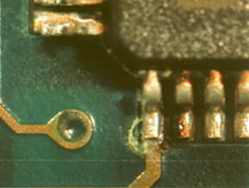
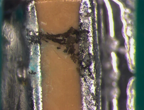
2. Inspection and Preventive Maintenance
Regular inspections help detect early signs of damage, corrosion, or wear.
2.1 Visual Inspection
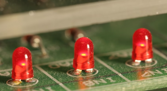
- Solder Joints – Look for cracks, cold joints, or discoloration.
- Traces & Pads – Check for corrosion, burns, or broken connections.
- Components – Inspect for bulging capacitors, burnt resistors, or loose parts.
2.2 Electrical Testing
- Multimeter Checks – Test for continuity, shorts, and open circuits.
- Thermal Imaging – Detect overheating components.
- Functional Testing – Verify PCB operation in real-world conditions.
2.3 Corrosion Prevention
- Conformal Coating – Apply acrylic, silicone, or urethane coatings to protect against moisture and oxidation.
- Desiccant Packs – Store PCBs in dry environments with silica gel to absorb moisture.
- Gold-Plated Contacts – Use gold-plated connectors where possible to resist corrosion.
3. Environmental Control
PCBs are sensitive to environmental factors such as humidity, temperature, and static electricity.
3.1 Humidity & Moisture Control
- Ideal Humidity: 30-60% RH (Relative Humidity).
- Moisture Protection:
- Use moisture barrier bags (MBBs) for storage.
- Bake moisture-sensitive PCBs (if exposed to high humidity) before reflow soldering.
3.2 Temperature Management
- Avoid Extreme Heat: Prolonged exposure above 85°C can degrade components.
- Thermal Cycling: Sudden temperature changes can cause solder joint fatigue.
3.3 ESD (Electrostatic Discharge) Protection
- Grounding Straps – Wear anti-static wrist straps when handling PCBs.
- ESD-Safe Workstations – Use conductive mats and grounded tools.
- Anti-Static Bags – Store and transport PCBs in shielded packaging.
4. Proper Handling & Storage
Improper handling can cause physical damage, while poor storage leads to environmental degradation.
4.1 Handling Best Practices
- Avoid Touching Traces & Pins – Skin oils can cause corrosion.
- Use Proper Tools – Tweezers, vacuum pickers, and non-metallic tools prevent damage.
- Minimize Flexing – Bending PCBs can crack traces or solder joints.
4.2 Storage Guidelines
- Temperature & Humidity Control – Store in a climate-controlled environment.
- Vertical Storage – Stack PCBs vertically in anti-static holders to prevent warping.
- Avoid Direct Sunlight – UV exposure can degrade solder masks and components.
5. Repair & Rework Techniques
Even with proper maintenance, PCBs may require repairs. Follow best practices to avoid further damage.
5.1 Soldering & Desoldering
- Use Temperature-Controlled Irons – Prevent overheating.
- Solder Suction Tools – Remove excess solder without damaging pads.
- Flux Application – Improves solder flow and reduces oxidation.
5.2 Component Replacement
- Match Specifications – Replace faulty components with identical or superior ratings.
- Reflow Soldering – For SMD components, use a rework station with precise temperature control.
5.3 Trace Repair
- Conductive Epoxy or Wire Jumps – Repair broken traces carefully.
- Test Continuity – Ensure repairs restore proper electrical connections.
6. Long-Term PCB Care
For PCBs in long-term storage or infrequent use:
- Periodic Power-Up – Prevents capacitor degradation (especially electrolytic capacitors).
- Reapply Conformal Coating – If stored in harsh environments.
- Document Maintenance Logs – Track inspections, cleanings, and repairs.
Conclusion
Proper PCB maintenance extends the lifespan of electronic devices, reduces failure rates, and ensures reliable performance. By following systematic cleaning, inspection, environmental control, and handling procedures, technicians and engineers can prevent common PCB issues such as corrosion, overheating, and mechanical damage. Implementing these best practices will optimize PCB functionality and reduce costly repairs or replacements in the long run.
By adhering to these guidelines, businesses and hobbyists alike can maximize the efficiency and durability of their electronic systems.