Proper PCB Grounding for Mixed-Signal Designs
Mixed-signal PCB design grounding issues can be avoided by paying attention to where current flows. In this tutorial, we will show how ground plane cuts and multiple mixed-signal ICs can solve grounding issues and crosstalk problems. We will also discuss the basic concepts of current flow, signal routing, and how to place components.
Mixed-signal PCB design grounding issues can be avoided by paying attention to where current flows. In this tutorial, we will show how ground plane cuts and multiple mixed-signal ICs can solve grounding issues and crosstalk problems. We will also discuss the basic concepts of current flow, signal routing, and how to place components.
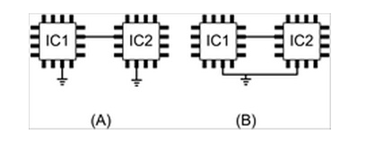
Board-level designers often worry about the proper way to handle grounding for integrated circuits (ICs) because integrated circuits have separate analog and digital grounds. Should the two be completely separate and never touch? Should they be connected at a single point where there is a cut in the ground plane to enforce that single-point or “Mecca” ground? How can Mecca grounding be achieved when there are multiple ICs that require both analog and digital grounds?
Follow the Current Please
Remember, we refer to a collection of connected electrical or electronic components as a “circuit” because current always flows from a source to a load and then back through a return path (a loop of sorts). Remembering the direction of current flow, either in the direction to do the work required or in the return current that ends up being the current, is fundamental to making any analog circuit work properly. Yes, all digital circuits are analog circuits; they are a subset to which we assign meaning to only two states. The transistors and other components, as well as the currents and voltages within the circuit, still operate according to the same physical principles as other analog circuits. They will sense the return current in the same way as any other circuit.
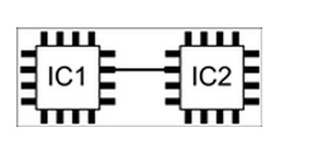
The simple connection is a direct connection from one IC to another.
Figure 1 shows the simplest connection in a design: a direct connection from one chip to another. As an ideal circuit in an ideal world, IC1 has zero output impedance and IC2 has infinite input impedance. Therefore, no current will flow. In the real world, however, current will flow from IC1 to IC2, or vice versa. What happens to this current? Does it just fill up IC2 or IC1? That’s a funny rhetorical question.
In reality, there must be another connection between IC1 and IC2 to allow the current flowing from IC1 into IC2 to return to IC1 and vice versa. This connection is usually to ground and is not usually indicated in the digital portion of the schematic (Figure 1). It is often implied by the use of a ground symbol, ? ? as shown in Figure 2A. Figure 2B shows the complete current circuit.

The simple circuit of Figure 1 implies ground (2A) and indicates the ground current path (2B).
Of course, the IC itself is not the current source. The power supply to this circuit is. For simplicity, we assume there is only one power rail and treat the power supply as a battery. For completeness, we bypass the power supply to the IC with a capacitor.
All DC currents eventually start and end at the power supply. Figure 3 shows the complete circuit for DC current when IC1 is providing the current shown.
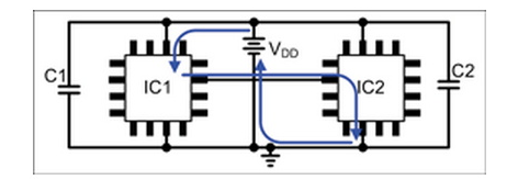
IC1 sources DC current.
For high-frequency signals (“high” is determined primarily by the bypass capacitor and the source impedance), the current starts and ends at the bypass capacitor. Figure 4 shows the high-frequency signal current.
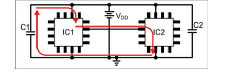
IC1 sources high-frequency signal current.
It is important to remember that the output is not always a current source. For example, consider the case where the output of IC1 is connected to the input of IC2, which has a pull-up resistor connected to VDD.