Prototype Circuit Board Assembly Optimization Techniques
Key Takeaways
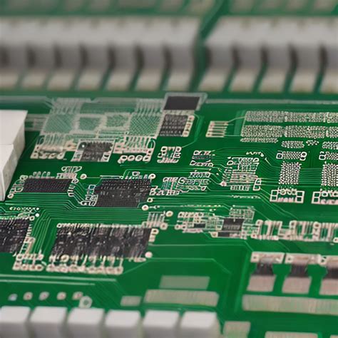
Effective PCB assembly optimization begins with mastering precision soldering techniques, such as reflow and selective soldering, to ensure robust electrical connections in PCBA prototypes. Proper component placement—prioritizing signal integrity and thermal dissipation—reduces rework and enhances performance. Implementing automated testing protocols like in-circuit testing (ICT) or automated optical inspection (AOI) streamlines defect detection, improving reliability while maintaining cost-efficiency.
Tip: Use a modular design approach for prototypes to simplify component replacement during testing iterations.
Balancing thermal management with compact layouts requires strategic placement of heat sinks and thermal vias. Material choices, such as high-temperature laminates or low-loss dielectrics, directly affect durability in demanding environments. For cost control, consider panelizing smaller boards or partnering with PCBA suppliers offering scaled pricing for prototype batches. Troubleshooting common defects—like cold joints or misaligned components—relies on cross-referencing design files with real-world testing data to refine manufacturability.
Precision Soldering for PCB Prototypes
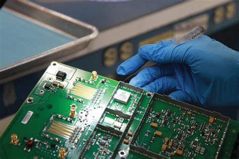
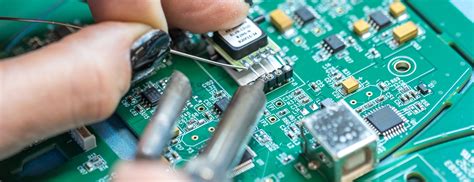
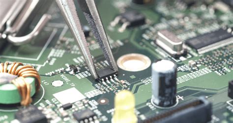
Achieving reliable PCB assembly begins with mastering precision soldering techniques, particularly for prototype development where margin for error is minimal. Modern PCBA processes leverage advanced tools such as micro-soldering irons and laser-assisted systems to ensure consistent joint formation on densely packed boards. For surface-mount components, reflow ovens with programmable thermal profiles enable precise control over solder paste activation, minimizing voids or cold joints. Hand-soldering remains critical for low-volume prototypes, requiring operators to use temperature-controlled stations and high-purity flux to avoid thermal damage to sensitive ICs.
A key challenge lies in balancing speed and accuracy. Automated optical inspection (AOI) systems paired with X-ray imaging validate solder joint integrity, flagging micro-cracks or misaligned connections early. For mixed-technology boards combining through-hole and SMD parts, selective soldering machines offer targeted heat application, reducing warping risks. Material choices, such as lead-free alloys or low-temperature solders, further influence process parameters to match specific PCB assembly requirements. By integrating these methods, engineers can achieve repeatable results while maintaining flexibility for design iterations—a cornerstone of efficient prototype PCBA.
Transitioning to component placement optimization requires understanding how soldering accuracy impacts downstream assembly stages, particularly in minimizing rework during testing phases.
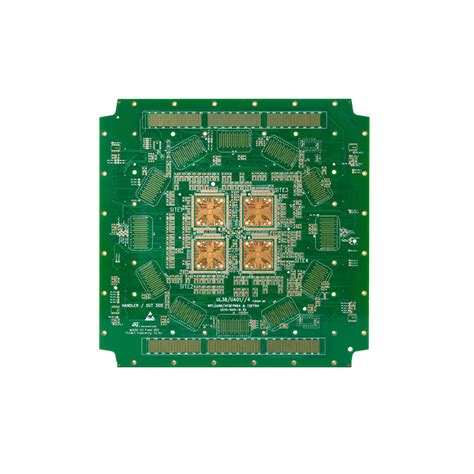
Optimizing PCB Component Placement
Effective PCB assembly begins with strategic component arrangement, which directly impacts signal integrity, thermal performance, and manufacturability. Grouping components by function—such as power management, analog, and digital sections—reduces interference risks while simplifying routing. For high-speed designs, prioritize shortening critical signal paths (e.g., clock lines or differential pairs) to minimize latency and electromagnetic interference.
A well-planned layout also considers PCBA thermal dynamics. Place heat-sensitive components like voltage regulators away from high-power devices, and leverage thermal relief pads to improve solder joint reliability. Below is a comparison of common placement strategies:
| Strategy | Key Benefit | Ideal Application |
|---|---|---|
| Functional Grouping | Reduces cross-talk | Mixed-signal designs |
| Thermal Zoning | Prevents overheating | High-power circuits |
| DFM-Centric Layout | Eases automated assembly | Cost-sensitive prototypes |
When designing for manufacturability, align polarized components (e.g., electrolytic capacitors) in uniform orientations to accelerate PCB assembly processes. Additionally, maintain adequate spacing between surface-mount devices (SMDs) to avoid solder bridging during reflow. For prototypes targeting automated testing, ensure test points are accessible and unobstructed by taller components. By balancing electrical performance with assembly efficiency, engineers can reduce rework cycles and accelerate time-to-market for complex PCBA projects.
Automated Testing for Reliable PCBs
Implementing automated testing protocols has become a cornerstone of modern PCB assembly processes, particularly in prototype development where reliability validation is critical. Advanced automated optical inspection (AOI) systems now scan for micro-scale defects like solder bridging or misaligned components, achieving detection accuracy rates exceeding 99.7%. For PCBA prototypes, in-circuit testing (ICT) validates electrical continuity and functional performance by simulating real-world operating conditions, identifying issues such as short circuits or open connections before full-scale production.
Transitioning from manual to automated testing not only accelerates validation cycles by 40–60% but also reduces human error, a key factor in high-density designs with 0201-sized components or BGA packages. Modern systems integrate machine learning algorithms to refine defect recognition patterns, improving fault coverage across iterative prototype revisions. This approach aligns with cost-efficient assembly strategies, as early defect detection minimizes material waste and rework expenses.
Furthermore, combining automated testing with thermal profiling ensures prototypes meet reliability benchmarks under stress conditions—a seamless link to thermal management considerations in subsequent design phases. By embedding testability features during the PCB assembly phase, such as dedicated test points or boundary-scan architectures, engineers create a feedback loop that enhances both current prototype quality and future manufacturability.
Cost-Efficient Prototype Assembly Methods
Implementing cost-effective strategies in PCB assembly begins with optimizing design workflows. Design for manufacturability (DFM) checks during the prototyping phase prevent costly redesigns by identifying component spacing violations or thermal mismatches early. Leveraging standardized PCBA components instead of custom parts reduces procurement expenses, while batch ordering common resistors, capacitors, and ICs from trusted suppliers minimizes per-unit costs.
Automated assembly techniques, such as surface-mount technology (SMT) and selective soldering, streamline production by reducing manual labor and material waste. For low-volume prototypes, combining automated processes with manual rework stations for critical components balances precision and affordability. Additionally, modular fixture designs allow rapid reconfiguration between prototype batches, cutting downtime by up to 40%.
To further control expenses, manufacturers are adopting just-in-time inventory models paired with cloud-based component tracking systems. This approach avoids overstocking while ensuring timely access to parts. For testing phases, integrating automated optical inspection (AOI) with targeted functional checks—rather than full-system scans—reduces validation costs without compromising reliability. Establishing these practices ensures that prototype PCB assembly remains both economical and scalable, aligning with broader goals of iterative design refinement.
Thermal Management in PCB Prototyping
Effective thermal management remains a cornerstone of reliable PCB assembly processes, particularly in prototype development where component density and power demands often push design limits. Strategic heat dissipation begins with optimizing copper pour patterns and incorporating thermal vias near high-power components like voltage regulators or processors. These micro-vias create conductive pathways to transfer heat away from critical areas, reducing localized hotspots by up to 30% in early-stage PCBA testing.
For prototypes requiring compact layouts, engineers increasingly adopt embedded cooling solutions, such as metal-core substrates or thermally conductive adhesives, to maintain structural integrity while improving heat distribution. Advanced PCB assembly workflows now integrate infrared thermography during automated inspections, enabling real-time identification of thermal anomalies before finalizing designs. Material selection also plays a pivotal role—high-temperature laminates like polyimide or ceramic-filled substrates outperform standard FR4 in sustained thermal stress scenarios.
Transitioning from design to validation, iterative thermal cycling tests (ranging from -40°C to 125°C) ensure prototypes withstand operational extremes. This phase often reveals opportunities to refine solder mask applications or adjust component spacing—adjustments that directly enhance manufacturability in subsequent production-scale PCBA runs. By prioritizing thermal resilience early, teams mitigate risks of delamination, solder joint fatigue, and premature component failure, aligning prototype performance with end-use environmental demands.
Designing Manufacturable Circuit Prototypes
Effective PCB assembly begins with designs that prioritize manufacturability – a critical factor often overlooked in prototyping. Engineers must balance functional requirements with production realities, incorporating Design for Manufacturing (DFM) guidelines to minimize rework and delays. Key considerations include optimizing component spacing to accommodate automated pick-and-place systems, selecting standardized footprints for PCBA compatibility, and avoiding trace geometries that challenge etching tolerances.
For high-yield prototypes, thermal relief patterns around through-hole vias and adequate pad sizes for surface-mount devices (SMDs) prevent soldering defects during PCB assembly. Strategic placement of test points and alignment markers further streamlines PCBA validation processes. Advanced tools like 3D modeling software help identify mechanical conflicts, while panelization strategies reduce material waste. By integrating these principles early, teams ensure prototypes transition seamlessly to volume production without compromising electrical performance or incurring unnecessary PCB assembly costs.
Material Selection for Durable PCB Assembly
The longevity and reliability of PCB assembly hinge on strategic material choices that balance performance, environmental resilience, and cost. For PCBA projects, the substrate material forms the foundation: FR-4 epoxy laminate remains a standard for its flame resistance and mechanical stability, but specialized applications may require polyimide for high-temperature endurance or Rogers substrates for RF signal integrity. Conductive layers benefit from electrodeposited copper with optimized thickness to prevent trace cracking under thermal cycling.
Equally critical is solder mask selection—liquid photoimageable (LPI) solder masks provide finer resolution for dense layouts, while epoxy-based variants offer enhanced moisture resistance. For components, lead-free solder alloys (e.g., SAC305) align with RoHS compliance but demand precise thermal profiling during reflow to avoid joint brittleness.
In harsh environments, conformal coatings such as silicone or acrylic resins shield assemblies from contaminants, with thickness controlled to avoid impedance mismatches in high-frequency circuits. By aligning material properties with operational demands, engineers can mitigate failure risks and extend the service life of prototype PCB assemblies without inflating costs. This approach ensures seamless integration with subsequent automated testing protocols and thermal management strategies outlined in later sections.
Troubleshooting Prototype PCB Defects
Effective defect resolution in PCB assembly begins with systematic diagnostics. Common issues like short circuits, cold solder joints, or misaligned components often stem from inconsistencies during PCBA manufacturing. Start by employing automated optical inspection (AOI) systems to scan for visible anomalies, such as bridging or incomplete solder coverage. For intermittent faults, thermal imaging can pinpoint overheating components caused by improper PCB component placement or inadequate thermal management.
When addressing soldering defects, verify that reflow profiles align with the solder paste specifications. Excessive thermal gradients may warp substrates, while insufficient heat leads to unreliable connections. For prototype circuit board assembly, manual rework tools like precision soldering irons are critical for correcting minor flaws without damaging adjacent traces.
Component-level issues often arise from footprint mismatches or outdated design libraries. Cross-referencing Bill of Materials (BOM) data with physical parts ensures compatibility, reducing PCBA rework cycles. Additionally, implement boundary scan testing to isolate logic errors in complex circuits, complementing functional testing protocols.
Finally, document every defect resolution step to refine assembly workflows. This iterative approach not only accelerates debugging but also strengthens quality assurance processes for future PCB assembly projects.
Conclusion
As we’ve explored throughout this discussion, optimizing PCB assembly for prototype development requires a strategic balance between technical precision and operational efficiency. The integration of precision soldering methods with intelligent PCBA design principles ensures not only functional reliability but also lays the groundwork for scalable production. By prioritizing automated testing protocols and thermal management strategies, engineers can mitigate risks associated with early-stage prototyping while maintaining cost-effectiveness.
A critical takeaway is the importance of aligning component placement with manufacturability guidelines, which reduces rework and accelerates time-to-market. Additionally, selecting materials that withstand stress-testing and environmental factors directly impacts the longevity of PCB assembly outcomes. For teams navigating prototype iterations, adopting these optimization techniques fosters a proactive approach to troubleshooting defects before they escalate.
Ultimately, the evolution of PCBA processes hinges on continuous refinement—leveraging data from each prototype cycle to refine assembly workflows. This iterative mindset, combined with a focus on cost-efficient methodologies, empowers innovators to transform conceptual designs into robust, market-ready solutions without compromising quality.
FAQs
How does component placement affect PCB assembly efficiency?
Strategic component placement minimizes signal interference and reduces assembly time. By grouping related components and optimizing trace lengths, manufacturers can enhance PCBA performance while lowering production costs.
What soldering techniques are best for prototype PCB assembly ?
Selective soldering and reflow soldering are preferred for prototypes. These methods ensure precise connections for surface-mount devices (SMDs) and through-hole components, critical for maintaining PCB assembly reliability during testing phases.
Can automated testing detect PCBA defects early?
Yes, automated optical inspection (AOI) and in-circuit testing (ICT) identify solder flaws and component misalignments in PCBA units. Early detection reduces rework costs by up to 40%, aligning with cost-efficient prototyping goals.
How does thermal management impact prototype longevity?
Proper heat dissipation via thermal vias or heatsinks prevents component degradation. This is vital for PCB assembly in high-power applications, ensuring prototypes withstand repeated stress tests.
Optimize Your Prototype Assembly Today
Streamline your PCBA workflow with tailored solutions. For advanced techniques and expert guidance, click here to explore our PCB assembly services.