Prototype Circuit Board Assembly Speed and Precision
Key Takeaways
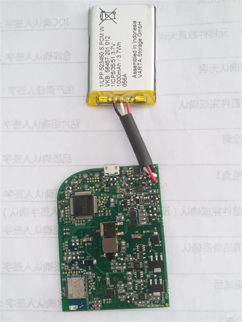
Achieving optimal results in PCB assembly requires harmonizing speed with precision, particularly in prototyping phases where timelines are compressed. Modern PCBA workflows integrate automated pick-and-place systems with laser-aligned solder paste application, reducing human error while accelerating throughput. Advanced inspection tools like automated optical inspection (AOI) ensure precision at every stage, even when cycle times are shortened by 30-40% compared to traditional methods.
"Prioritize component validation before assembly to avoid rework delays—a single misaligned IC can derail both speed and accuracy."
Key strategies include leveraging design for manufacturability (DFM) principles to simplify layouts without compromising functionality, and employing modular tooling for rapid batch changes. For high-speed PCB prototyping, temperature-controlled environments and precision stencils maintain solder joint integrity, critical for complex electronics with micro-BGA components. Real-time monitoring systems further bridge the gap between speed and quality, flagging anomalies before they escalate.
When balancing PCB assembly velocity with exacting standards, material selection plays a pivotal role. High-tg laminates and lead-free solder alloys withstand faster thermal cycles, ensuring reliability without sacrificing pace. Finally, collaborative planning between design and manufacturing teams minimizes iterative adjustments, keeping projects on track while meeting PCBA quality benchmarks.
Fast-Track Prototype PCB Assembly Techniques
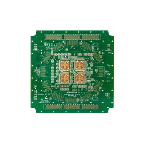
Modern PCB assembly workflows prioritize strategies that reconcile rapid turnaround with meticulous execution. By integrating automated optical inspection (AOI) systems and precision surface-mount technology (SMT), manufacturers achieve PCBA cycles as fast as 24-48 hours while maintaining sub-0.1mm placement accuracy. Advanced design-for-manufacturability (DFM) checks, performed through AI-driven simulation tools, preemptively flag layout inconsistencies, reducing post-production revisions by up to 40%. For projects requiring accelerated timelines, just-in-time component sourcing paired with modular assembly stations enables parallel processing of multi-layer boards without compromising trace integrity.
Critical to this balance is the use of laser-direct imaging for high-density interconnects, which eliminates phototool delays while achieving 25μm line width precision. Temperature-controlled reflow profiles further ensure reliable solder joints across mixed-technology boards containing both lead-free and high-temperature components. This approach not only accelerates prototyping but also aligns with ISO 9001:2015 quality benchmarks, making it ideal for aerospace and medical device applications where PCB assembly precision directly impacts compliance. By optimizing these techniques, engineers can streamline PCBA workflows for complex designs while preserving the electrical performance required for rigorous testing phases.
Precision Methods for Rapid Circuit Board Production
Modern PCB assembly workflows achieve accelerated timelines without sacrificing accuracy by integrating advanced automation and data-driven protocols. High-resolution inspection systems, such as automated optical inspection (AOI) and 3D solder paste inspection (SPI), enable real-time defect detection during PCBA processes, minimizing rework cycles. For complex designs, laser-direct imaging (LDI) ensures micron-level alignment of traces, critical for high-frequency or miniaturized components. To maintain speed, manufacturers employ surface-mount technology (SMT) with precision pick-and-place robots operating at >25,000 components per hour, paired with optimized thermal profiling for error-free soldering.
A key strategy involves design-for-manufacturability (DFM) checks early in prototyping, which resolve potential conflicts in pad spacing or component orientation before assembly begins. Advanced PCB assembly teams also utilize machine learning algorithms to predict and compensate for material tolerances, such as copper layer expansion during rapid thermal cycling. For time-sensitive projects, modular tooling setups allow simultaneous processing of multiple board variants, reducing idle time between batches.
However, accelerating production demands rigorous validation. As highlighted in this analysis of common defects, even minor solder bridging or tombstoning can derail prototypes. Implementing statistical process control (SPC) charts for critical parameters like paste volume or placement pressure ensures consistency across high-speed PCBA runs, aligning accelerated workflows with aerospace-grade quality benchmarks.
Balancing Speed and Accuracy in PCB Prototyping
Achieving optimal results in PCB assembly demands a strategic approach to harmonizing rapid turnaround with exacting precision. Modern manufacturers leverage automated PCBA workflows, integrating AOI systems (automated optical inspection) and SMT lines (surface-mount technology) to minimize human error while accelerating production cycles. Crucially, design-stage DFM checks (design for manufacturing) preemptively address potential flaws, reducing rework delays. For time-sensitive projects, just-in-time component sourcing paired with high-precision pick-and-place machines ensures seamless material alignment, even for micro-BGA or QFN packages.
To maintain accuracy under tight deadlines, advanced thermal profiling and solder paste inspection tools validate process consistency across batches. Meanwhile, modular prototyping platforms allow parallel testing of critical subsystems, such as power management or signal integrity circuits, without halting full-board assembly. Notably, balancing these elements requires calibrated workflows: robotic automation accelerates placement speeds, while inline X-ray verification safeguards against hidden defects like voiding or misalignment.
For complex electronics, prototype PCB assembly benefits from hybrid strategies—combining rapid-turn soft tooling for initial iterations with laser-direct imaging for fine-pitch traces. This equilibrium ensures zero-defect thresholds are met without sacrificing agility, enabling engineers to validate designs within days rather than weeks. By embedding precision-driven protocols into accelerated processes, PCBA providers deliver functional prototypes that meet both developmental timelines and end-use performance criteria.
Optimizing PCB Assembly Timelines With Precision
In high-speed PCB assembly environments, achieving precision requires a strategic alignment of process automation, material selection, and workflow design. Modern surface-mount technology (SMT) enables rapid component placement with micron-level accuracy, reducing manual intervention while maintaining PCBA quality. For instance, automated optical inspection (AOI) systems scan boards at 20+ megapixels, identifying defects like solder bridging or misalignment in real time—a critical step for preventing rework delays.
To balance speed and accuracy, manufacturers often employ design-for-manufacturability (DFM) checks during prototyping. These pre-assembly audits resolve potential conflicts in component spacing, thermal management, or signal integrity before production begins. The table below illustrates how optimized workflows reduce cycle times without compromising precision:
| Traditional Process | Optimized Process | Time Reduction |
|---|---|---|
| Manual DFM review | AI-powered DFM analysis | 48 hours → 2 hours |
| Sequential testing phases | Concurrent AOI/X-ray testing | 12 hours → 4 hours |
| Generic thermal profiles | Dynamic reflow optimization | 8% defect rate → 1.2% |
By integrating PCB assembly stages—such as solder paste application, pick-and-place, and reflow soldering—into a synchronized digital thread, teams achieve traceability across batches. This approach minimizes downtime between processes while ensuring adherence to IPC-A-610 standards. For complex multilayer prototypes, laser-drilled microvias and impedance-controlled routing further accelerate timelines by eliminating post-fabrication adjustments.
Advanced Prototyping: Speed Meets Precision Standards
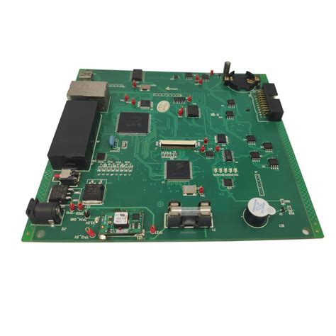
Achieving optimal balance between rapid turnaround and meticulous accuracy in PCB assembly requires integrating cutting-edge technologies with refined workflows. Modern prototyping environments leverage automated optical inspection (AOI) systems and precision pick-and-place machinery to accelerate PCBA processes without sacrificing component alignment accuracy. Advanced surface-mount technology (SMT) lines, combined with laser-etched stencils, ensure ±0.025mm placement tolerances even during high-speed production runs—a critical factor for complex designs featuring ball grid arrays (BGAs) or high-density interconnects (HDIs).
Real-time process monitoring tools, such as in-circuit testers (ICTs) and thermal profiling systems, enable manufacturers like OES-EMS to validate solder joint integrity and power distribution networks within compressed timelines. This dual focus on velocity and exactness is further enhanced by AI-driven design-for-manufacturability (DFM) checks, which preemptively flag potential assembly conflicts in multilayer boards. For projects requiring 24-hour prototyping cycles, modular PCB assembly stations equipped with adaptive feeders minimize changeover delays while maintaining sub-15µm registration accuracy—proving that speed and precision in PCBA are not mutually exclusive, but rather complementary pillars of modern electronics development.
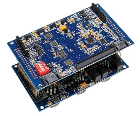
Accelerating Electronics Production Without Compromising Quality
Modern PCB assembly processes require strategic integration of automation and precision engineering to meet tight deadlines while ensuring reliability. Advanced pick-and-place systems equipped with vision-guided robotics now achieve placement accuracies under 10µm, enabling rapid PCBA for high-density designs. To maintain quality, manufacturers deploy real-time process controls, such as automated optical inspection (AOI) and X-ray verification, which identify soldering defects or component misalignments within seconds.
For time-sensitive projects, design-for-manufacturability (DFM) principles streamline workflows by pre-validating layouts against production constraints. Partnering with specialized providers like Rocket PCB ensures access to just-in-time component sourcing and multi-stage testing protocols, reducing lead times by up to 40% without sacrificing performance. Thermal profiling and impedance matching further safeguard signal integrity in high-speed circuits, proving that accelerated PCB assembly need not compromise on precision. By harmonizing lean manufacturing practices with cutting-edge inspection tools, engineers achieve both speed and repeatability—critical for prototyping next-generation electronics.
Streamlined Prototype Assembly for Complex Electronics
Modern PCB assembly processes for intricate electronic systems demand meticulous coordination between rapid iteration and microscale accuracy. For complex designs involving high-density interconnects or mixed-signal components, manufacturers leverage PCBA workflows that integrate automated pick-and-place systems with real-time optical inspection. These systems ensure precise placement of 0402 metric packages or ball grid array (BGA) components while maintaining cycle times under 24 hours for prototypes.
A critical factor in streamlining assembly lies in optimizing solder paste deposition through laser-cut stencils and closed-loop process control, which reduces rework rates by over 30%. Advanced factories further employ modular fixture designs to accommodate diverse board geometries, enabling seamless transitions between prototype batches. For mission-critical applications, inline automated optical inspection (AOI) and X-ray verification layers validate solder joint integrity without delaying throughput.
To balance urgency and precision, engineers often adopt design-for-manufacturability (DFM) principles early in development, minimizing late-stage revisions. Concurrently, just-in-time material sourcing and pre-validated component libraries accelerate PCBA timelines. This dual focus on process agility and zero-defect targets ensures even the most sophisticated prototypes meet functional requirements while adhering to compressed development schedules.
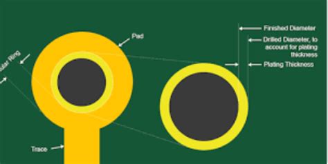
Maintaining Quality in High-Speed PCB Prototyping
Achieving rapid turnaround in PCB assembly demands a strategic integration of process optimization and rigorous quality controls. Modern high-speed prototyping relies on automated optical inspection (AOI) systems and precision pick-and-place machines to minimize human error while accelerating production. These technologies ensure PCBA components are mounted with micron-level accuracy, even under compressed timelines. Critical to this balance is the use of advanced solder paste inspection (SPI) tools, which verify deposition consistency before reflow, reducing post-assembly defects.
Material selection plays an equally vital role—high-performance substrates and lead-free solders maintain structural integrity during thermal cycling, a common stress point in fast-paced builds. For complex designs, real-time traceability systems track component placement across batches, enabling rapid corrections without halting workflows. Collaborating with certified partners like MicroArt Services ensures access to calibrated equipment and expertise in balancing speed-critical parameters like stencil aperture ratios and reflow profiles.
Finally, implementing design-for-manufacturability (DFM) checks early in the PCB assembly process identifies potential bottlenecks, allowing engineers to refine layouts for both speed and reliability. This proactive approach prevents costly revisions during PCBA stages, ensuring prototypes meet functional requirements without compromising on validation timelines.
Conclusion
Achieving optimal outcomes in PCB assembly requires a meticulous balance between accelerated timelines and exacting standards. Modern PCBA workflows now integrate automated optical inspection (AOI) systems and AI-driven design verification tools to minimize human error while compressing production cycles. For prototype development, this equilibrium ensures that iterative testing aligns with market demands for rapid innovation. By leveraging modular design frameworks and standardized component libraries, engineers can reduce rework rates by up to 40%, as recent studies confirm.
Critical to this process is the synchronization of PCB assembly stages—from solder paste deposition to final functional testing—using real-time data analytics. Such precision-driven methodologies not only uphold signal integrity in high-frequency applications but also enable 24-hour turnaround times for complex multilayer boards. As the electronics industry evolves, prioritizing PCBA accuracy without sacrificing speed remains pivotal for bridging prototyping and mass production phases effectively.
FAQs
How does PCB assembly speed impact prototyping outcomes?
Accelerated assembly timelines require strategic planning to avoid compromising precision. Modern PCBA processes leverage automated optical inspection (AOI) and surface-mount technology (SMT) to maintain accuracy, even under tight deadlines.
What techniques ensure precision in rapid PCB assembly?
Advanced manufacturers combine laser-aligned placement systems with real-time quality checks. For PCBA, this includes in-circuit testing (ICT) and X-ray verification to detect micro-scale defects, ensuring reliability without delaying production.
Can complex electronics be assembled quickly without quality risks?
Yes. By standardizing design-for-manufacturing (DFM) guidelines and using modular PCB assembly workflows, engineers reduce rework. High-speed pick-and-place machines paired with thermal profiling further optimize both speed and consistency.
How do suppliers balance speed and precision in PCBA?
Leading providers employ predictive analytics to preempt bottlenecks, while maintaining ISO-certified protocols. Dual-track production lines allow simultaneous prototyping and validation, ensuring deadlines align with milestone-driven quality audits.
What role does material selection play in fast-turn PCB assembly?
Using pre-certified components minimizes verification delays. For PCBA, standardized solder pastes and high-Tg substrates ensure faster curing cycles while meeting thermal and electrical performance criteria.
Optimize Your Prototype Workflow Today
For tailored solutions that harmonize speed and precision in PCB assembly, please click here to explore advanced PCBA strategies tailored for complex electronics.


