Prototype PCB Assembly Strategies for Accelerated Product Development

Key Takeaways
Effective PCB assembly strategies are pivotal for accelerating product development cycles while maintaining rigorous quality benchmarks. By integrating precision manufacturing processes and rapid turnaround tactics, teams can reduce prototyping timelines by up to 40%, according to industry studies.
Tip: Prioritize suppliers offering PCBA-specific expertise, as their familiarity with high-mix, low-volume production ensures fewer design revisions and faster iteration cycles.
Three core elements define successful prototyping:
- Collaborative Supplier Partnerships: Aligning with PCB assembly providers that offer real-time feedback loops minimizes errors in component sourcing and placement.
- Automated Validation Tools: Leveraging AI-driven inspection systems reduces post-assembly testing time by 25–30%.
- Design-for-Manufacturability (DFM): Optimizing layouts for PCBA compatibility cuts rework risks and accelerates scalability.
| Traditional Approach | Accelerated Strategy |
|---|---|
| 4–6-week lead times | 7–10-day rapid PCBA |
| Manual quality checks | In-line AOI/X-ray verification |
| Fixed BOM requirements | Flexible component substitution |
Balancing speed and quality requires adopting modular prototyping frameworks. For instance, using pre-validated PCB assembly subassemblies slashes integration delays by standardizing critical interfaces.
"Accelerated prototyping isn’t just about faster machines—it’s about synchronizing design, PCBA, and validation into a single feedback-driven workflow." – Industry Expert
By embedding these strategies, teams achieve first-pass success rates above 85%, ensuring prototypes meet both functional and compliance requirements before mass production.
Prototype PCB Assembly Accelerates Product Development
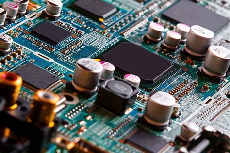
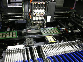
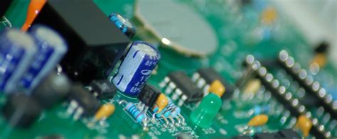
Integrating PCB assembly services early in the design phase significantly shortens development timelines by enabling rapid validation of electronic concepts. Modern prototyping workflows leverage PCBA (printed circuit board assembly) to transform schematic designs into functional units within days, bypassing traditional manufacturing delays. By aligning with suppliers specializing in low-volume, high-mix production, teams gain access to precision manufacturing tools like automated pick-and-place systems and 3D solder paste inspection—critical for minimizing rework.
The agility of prototype PCB assembly stems from optimized processes such as panelization for batch testing and just-in-time component sourcing, which reduce lead times by up to 60%. Real-time collaboration with assembly partners further ensures design-for-manufacturability (DFM) feedback loops, addressing potential flaws before mass production. This approach not only accelerates iteration cycles but also maintains compliance with industry quality standards, preventing costly mid-project revisions.
Advanced PCBA providers now combine rapid-turn fabrication with in-house testing suites, allowing concurrent validation of power integrity and signal performance. Such integration ensures that prototypes mirror final-product behavior, enabling faster certification and market entry. For startups and enterprises alike, strategic use of PCB assembly services bridges the gap between concept and commercialization, turning months-long timelines into weeks without compromising reliability.
Optimizing Prototyping Cycles With PCB Strategies
Effective PCB assembly strategies are pivotal in shortening prototyping timelines without compromising functionality. By integrating design for manufacturability (DFM) principles early in the development phase, engineers can preemptively address potential bottlenecks in PCBA workflows. For instance, selecting standardized components reduces sourcing delays, while modular design practices enable iterative testing of critical subsystems.
Leveraging rapid-turn fabrication services for PCB assembly ensures that design revisions are implemented within days, accelerating feedback loops. Advanced manufacturers often combine automated solder paste application with high-speed pick-and-place systems to maintain consistency across low-volume prototype batches. This approach minimizes rework and aligns with agile development frameworks, where quick iterations are essential.
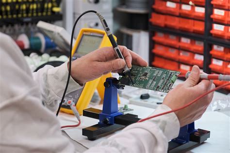
Collaboration with PCBA partners further streamlines cycles. Sharing real-time design files and test protocols allows suppliers to align their processes with project milestones. For example, in-circuit testing (ICT) and functional validation can be conducted in parallel with enclosure design, reducing idle time between phases. Such synchronization ensures that prototypes meet both performance benchmarks and regulatory requirements early in the cycle.
To maintain momentum, teams should prioritize traceability in PCB assembly workflows. Detailed documentation of material lots and assembly parameters simplifies root-cause analysis if defects arise, preventing prolonged delays. By balancing speed with systematic validation, companies can transform prototyping from a bottleneck into a catalyst for innovation.
Precision Manufacturing for Faster Product Launches
Achieving rapid product launches hinges on precision manufacturing practices that minimize errors and eliminate costly rework cycles. Modern PCB assembly processes leverage automated pick-and-place systems, laser-aligned soldering, and high-resolution inspection tools to ensure micron-level accuracy in component placement. By integrating PCBA (Printed Circuit Board Assembly) workflows with CAD-driven prototyping, teams can detect design flaws at the earliest stages, reducing post-production modifications by up to 40%.
Critical to this approach is the synchronization of design for manufacturability (DFM) principles with fabrication timelines. Advanced manufacturers employ real-time process monitoring to maintain tight tolerances across solder paste application and thermal profiles, ensuring consistent quality even under accelerated schedules. For instance, combining PCB assembly with automated optical inspection (AOI) systems allows immediate verification of ball grid arrays (BGAs) and micro-BGA components, slashing validation time by 50% compared to manual checks.
Moreover, partnering with PCBA providers that offer concurrent engineering support enables cross-functional collaboration between design and production teams. This alignment not only accelerates material sourcing but also optimizes panelization strategies to maximize yield rates. Such precision-driven methodologies create a foundation for faster iteration cycles, ensuring prototypes meet performance benchmarks while keeping development timelines on track.
Rapid Turnaround Tactics in PCB Prototyping
Achieving rapid turnaround in PCB assembly requires a strategic blend of design optimization, process automation, and supply chain agility. By implementing design-for-manufacturability (DFM) checks early, engineers can minimize revisions during PCBA stages, reducing delays caused by rework. Leveraging automated pick-and-place systems and solder paste inspection (SPI) accelerates component placement while maintaining precision.
Collaborating with suppliers offering just-in-time (JIT) component sourcing ensures critical parts arrive synchronously with fabrication schedules, avoiding bottlenecks. Additionally, selecting PCB assembly partners with dedicated prototyping lines—rather than shared production facilities—enables prioritized scheduling for faster iteration cycles. Real-time communication tools, such as cloud-based project dashboards, further streamline feedback loops between design teams and manufacturers.
For ultra-fast turnarounds, some providers combine PCBA services with in-house testing, allowing functional validation within 24–48 hours post-assembly. This integrated approach eliminates third-party dependencies, compressing timelines without compromising quality. Balancing these tactics ensures prototypes meet aggressive development milestones while laying the groundwork for scalable production.
Supplier Collaboration Enhances Prototype Quality
Effective partnership with PCB assembly suppliers significantly elevates prototype reliability by aligning design intent with manufacturing capabilities. Early engagement with experienced PCBA providers enables engineers to address potential fabrication challenges during the design phase, reducing iterative delays. Suppliers offering real-time feedback on material compatibility, component sourcing, and thermal management contribute directly to first-pass success rates.
Proactive collaboration tools, such as shared design-for-manufacturability (DFM) platforms, ensure seamless communication between development teams and PCB assembly specialists. This integration allows for rapid adjustments to trace widths, layer stack-ups, or solder mask specifications before prototyping begins. Leading PCBA partners often maintain component libraries with verified footprints, accelerating BOM validation while minimizing layout errors.
Establishing clear quality benchmarks with suppliers—such as IPC-A-610 acceptance criteria or impedance control tolerances—creates a unified framework for prototype evaluation. Joint failure mode analysis further strengthens quality outcomes by correlating test results with process parameters. When suppliers operate as technical allies rather than transactional vendors, they become instrumental in balancing speed with precision across PCB assembly workflows.
Balancing Speed and Quality in PCB Assembly
Achieving equilibrium between PCB assembly velocity and reliability remains a critical challenge in prototyping. While accelerated timelines are essential for competitive product development, compromising on quality risks costly redesigns or field failures. Strategic planning in PCBA workflows begins with design for manufacturability (DFM) analysis, which identifies potential production bottlenecks early. For instance, optimizing component placement not only reduces assembly time but also minimizes soldering defects.
Leveraging automated optical inspection (AOI) systems ensures rigorous quality checks without delaying turnaround. However, balancing these checks requires collaboration with suppliers who provide real-time feedback on material availability and alternative components. A common pitfall lies in over-prioritizing speed: skipping thermal stress testing or iterative testing phases may save days initially but lead to months of revisions.
Advanced PCB assembly services now integrate predictive analytics to forecast delays, enabling teams to adjust schedules proactively. By aligning fabrication timelines with rigorous testing protocols, manufacturers maintain first-pass yield rates above 90% while meeting tight deadlines. This dual focus ensures prototypes meet functional requirements without succumbing to time-to-market pressures. Ultimately, a structured approach to PCBA—combining lean processes with precision validation—creates a sustainable framework for delivering high-quality prototypes within accelerated timelines.
Advanced Techniques for Efficient PCB Prototyping
Modern PCB assembly processes leverage cutting-edge methodologies to reduce prototyping timelines without compromising functionality. One critical advancement is the integration of automated optical inspection (AOI) systems, which enable real-time defect detection during PCBA manufacturing. These systems minimize manual verification, accelerating iterative testing cycles by up to 40%. Additionally, 3D-printed tooling for custom jigs and fixtures eliminates traditional machining delays, allowing engineers to validate designs within 48 hours.
Adopting surface-mount technology (SMT) with fine-pitch components further enhances precision, particularly for high-density interconnect (HDI) boards. Pairing this with rapid thermal profiling ensures optimal solder joint integrity, even under compressed timelines. To maintain alignment with broader product development goals, teams are increasingly utilizing design-for-manufacturability (DFM) software to preemptively address compatibility issues in PCB assembly workflows.
For time-sensitive projects, hybrid models combining partial panelization and batch processing optimize material usage while supporting parallel testing. This strategy reduces waste and enables simultaneous validation of multiple design variants. Crucially, embedding in-circuit testing (ICT) protocols directly into PCBA workflows ensures functional reliability at every stage, bridging the gap between rapid iteration and rigorous quality assurance. By integrating these techniques, engineers achieve a 30–50% reduction in prototyping phases, setting the stage for seamless transitions to scaled production.
Streamlining Development Through PCB Assembly
Effective PCB assembly processes serve as the backbone of modern prototyping, enabling teams to compress development timelines without compromising functionality. By integrating PCBA (printed circuit board assembly) workflows early in the design phase, engineers can identify potential bottlenecks, such as component placement conflicts or thermal management issues, before committing to full-scale production. This proactive approach minimizes costly redesigns and ensures that design iterations align with manufacturing realities.
Leveraging rapid-turnaround PCB assembly services allows teams to shorten feedback loops, with some suppliers delivering functional prototypes in as few as 24–48 hours. Advanced techniques like surface-mount technology (SMT) and automated optical inspection (AOI) further accelerate validation cycles by ensuring precise component alignment and solder joint integrity. For optimal results, organizations should prioritize suppliers offering design-for-manufacturability (DFM) feedback, which bridges gaps between theoretical designs and practical assembly constraints.
Collaborative tools, such as shared digital dashboards for PCBA status tracking, enhance transparency across cross-functional teams. By synchronizing design, procurement, and assembly phases, businesses reduce idle time and maintain momentum toward product launch milestones. This holistic approach to PCB assembly not only accelerates time-to-market but also establishes a foundation for scalable, high-volume manufacturing.
Conclusion
Effective PCB assembly strategies form the backbone of accelerated product development, bridging the gap between design validation and market readiness. By integrating precision manufacturing with PCBA processes, teams can minimize design iterations while ensuring functional reliability. Rapid prototyping workflows, supported by collaborative supplier partnerships, enable engineers to test concepts under real-world conditions without compromising quality benchmarks. The strategic balance of speed and technical rigor in prototype builds not only reduces time-to-market but also mitigates risks in scaling production.
As industries demand faster innovation cycles, leveraging advanced PCB assembly techniques—such as automated optical inspection and just-in-time component sourcing—ensures prototypes meet both performance and regulatory requirements. Furthermore, aligning PCBA timelines with cross-functional development stages creates a seamless transition from prototyping to mass manufacturing. By prioritizing iterative testing and transparent communication with suppliers, organizations can transform prototype phases into strategic advantages, ultimately driving competitive differentiation in dynamic markets.
Frequently Asked Questions
How does prototype PCB assembly differ from full-scale production?
PCB assembly for prototyping focuses on low-volume, high-precision builds to validate designs, whereas production prioritizes volume efficiency. Prototypes emphasize rapid turnaround and iterative testing, often requiring flexible PCBA workflows to accommodate design changes.
What strategies ensure quality in fast-paced prototyping cycles?
Implementing automated optical inspection (AOI) and partnering with suppliers offering concurrent engineering reduces errors. Prioritizing design for manufacturability (DFM) early streamlines PCB assembly, while certified PCBA providers maintain compliance with industry standards.
How can supplier collaboration accelerate development timelines?
Close coordination with PCB assembly partners enables real-time feedback on material availability and design adjustments. Suppliers with integrated PCBA services often provide component sourcing support, minimizing delays caused by supply chain bottlenecks.
What tools optimize design-to-prototype transitions?
Advanced software for signal integrity analysis and 3D board visualization helps preempt issues. Modular PCBA designs allow reusable sections, cutting rework time. Rapid prototyping technologies like laser drilling further compress timelines.
Are cost-effective prototypes possible without compromising performance?
Yes. Leveraging panelized designs for PCB assembly reduces material waste, while standardized component libraries in PCBA workflows lower sourcing costs. Balancing value engineering with critical performance metrics ensures affordability.
Ready to Accelerate Your Prototype Development?
Explore how our PCB assembly expertise can streamline your product launch. Click here to learn more about our rapid PCBA solutions and request a customized quote today.