Prototype PCB Fabrication: A Comprehensive Guide
Introduction
Printed circuit boards (PCBs) are a vital component in the design and development of modern electronic products. Whether it is consumer electronics, industrial equipment or medical devices, PCBs play a key role in connecting and supporting electronic components. The manufacture of prototype PCBs is an important part of the product development cycle. It can not only help engineers verify the feasibility of the design, but also find potential problems before the product is officially produced. This article will explore the manufacturing process, material selection, design considerations, and common challenges and solutions of prototype PCBs.
1.Definition of prototype PCBs
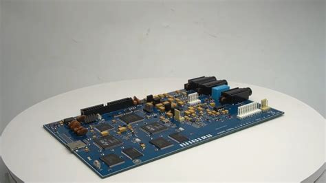
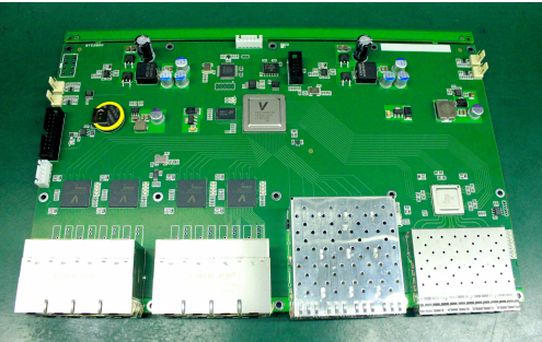
Prototype PCBs refer to circuit boards manufactured in the early stages of product development, mainly used to test and verify circuit designs. Compared with mass production PCBs, prototype PCBs usually have shorter delivery times and lower costs, and are suitable for rapid iteration and modification of designs. The main goal of prototype PCBs is to ensure the functionality and reliability of the design, laying the foundation for subsequent mass production.
2.Basic process of PCB manufacturing
The manufacturing process of PCBs usually includes the following steps:
2.1 Design
PCB design is the first step in prototype manufacturing. Designers use computer-aided design (CAD) software (such as Altium Designer, Eagle, KiCAD, etc.) to create circuit diagrams and PCB layouts. The design process needs to consider factors such as the function of the circuit, signal integrity, and thermal management.
2.2 Printing Circuit Diagrams
After the design is completed, the circuit diagram will be converted into a photomask file (Gerber file), which is a standard format for PCB manufacturing. Manufacturers make circuit boards based on these files.
2.3 Material Selection
The material selection of the prototype PCB has a great impact on its performance. Common PCB materials include:
FR-4: The most commonly used PCB substrate with good electrical insulation and mechanical strength.
High-frequency materials: used for radio frequency and microwave applications, with low dielectric constant and low loss characteristics.
Aluminum substrate: suitable for high-power applications, with good heat dissipation performance.
2.4 Making Circuit Boards
The manufacturing process includes the following steps:
Copper coating: Covering a layer of copper foil on the substrate.
Photolithography: Using photosensitive materials to form circuit patterns on the copper layer.
Etching: Remove excess copper, leaving the desired circuit pattern.
Drilling: Drill holes according to design requirements to install components and connect circuits.
Plating: Electroplate a layer of copper in the hole to ensure the conductivity of the circuit.
2.5 Surface treatment
In order to improve the solderability and corrosion resistance of the circuit board, PCBs usually need to be surface treated. Common surface treatment methods include:
HASL (hot air leveling): Tin solder is evenly applied to the surface of the circuit board by hot air.
Lead-free coating: Surface treatment is performed using lead-free materials to meet environmental standards.
2.6 Testing and verification
After the PCB is manufactured, electrical testing and functional verification are carried out to ensure that it meets the design requirements.
Common test methods include:
Functional testing: Check whether the circuit works as expected.
Signal integrity testing: Ensure that the signal is transmitted on the PCB without distortion.

3.Design considerations for prototype PCBs
When designing a prototype PCB, there are several key factors to consider:
3.1 Size and layout
The size and layout of the prototype PCB should be optimized according to the appearance and function of the final product. Reasonable layout can reduce signal interference and improve the reliability of the circuit.
3.2 Component selection
Choosing the right electronic components is the key to a successful design. Factors such as component size, power consumption and performance need to be considered.
3.3 Power management
Power management is an important part of PCB design. Designers need to ensure that power is distributed reasonably to avoid voltage drops and noise interference.
3.4 Heat dissipation design
For high-power applications, heat dissipation design is critical. Heat dissipation performance can be improved by adding heat sinks, optimizing layouts, etc.
3.5 Design rule check (DRC)
After the design is completed, a design rule check is performed to ensure that the PCB meets the manufacturer’s requirements. This includes checking line width, spacing, aperture, etc.

4.Challenges in Prototype PCB Manufacturing
Although the manufacturing process of prototype PCB is relatively simple, there are still some challenges:
4.1 Cost Control
The manufacturing cost of prototype PCB may be affected by materials, processes and delivery time. Engineers need to find a balance between performance and cost.
4.2 Time Pressure
In a fast-moving market, time to market is critical. Engineers need to shorten the manufacturing cycle of prototype PCB as much as possible to speed up the product development process.
4.3 Design Changes
Design changes are common in the prototype stage. Engineers need to respond to these changes flexibly and update design files in a timely manner.
4.4 Testing and Verification
Testing and verification are important links to ensure that PCB functions properly. Engineers need to develop detailed test plans to detect potential problems.
5.Future Development Trends
With the continuous advancement of technology, the manufacturing of prototype PCBs is also evolving. Future development trends include:
5.1 Automated Manufacturing
With the development of automation technology, the PCB manufacturing process will become more and more automated. This will improve production efficiency and reduce labor costs.
5.2 Additive Manufacturing (3D Printing)
The application of additive manufacturing technology will bring new possibilities to PCB manufacturing. Through 3D printing, more complex circuit structures and higher design flexibility can be achieved.
5.3 Environmentally friendly materials
With the increase of environmental awareness, PCB manufacturing will increasingly adopt environmentally friendly materials. This will help reduce the impact on the environment.
5.4 Intelligent Design
Intelligent design tools will help engineers design PCBs more quickly, automatically optimize layouts, and improve design efficiency.
Conclusion
The manufacture of prototype PCBs is an indispensable part of the electronic product development process. Through reasonable design, material selection, and manufacturing processes, engineers can quickly verify the feasibility of the design and lay the foundation for the successful launch of the product. Despite some challenges, with the continuous advancement of technology, the manufacture of prototype PCBs will become more efficient and intelligent. I hope this article can provide readers with valuable references and help the innovation and development of electronic products.


