PWB Assembly Advancements for Precision-Driven Manufacturing

Key Takeaways
Modern PCB assembly processes are undergoing transformative shifts driven by automation and material science breakthroughs. Central to this evolution is the integration of smart manufacturing systems, which leverage real-time data analytics to optimize PCBA workflows. Automated optical inspection (AOI) and robotic placement systems now achieve micron-level accuracy, reducing human error while accelerating production cycles.
Advancements in high-performance substrates and lead-free soldering alloys are enhancing thermal stability and signal integrity, critical for precision-driven applications. Concurrently, IoT-enabled quality control frameworks provide end-to-end traceability, flagging defects at subcomponent levels before final integration. These innovations align with sustainable practices, as manufacturers adopt energy-efficient equipment and recyclable materials to minimize environmental impact.
Emerging trends like AI-optimized assembly and additive manufacturing techniques further redefine PCB fabrication, enabling rapid prototyping and customization. By harmonizing data-driven decision-making with advanced PCBA technologies, the industry is poised to meet escalating demands for miniaturized, high-reliability electronics. This progression not only elevates production standards but also establishes a foundation for next-generation industrial IoT and 5G infrastructure.
Automated PWB Assembly Systems
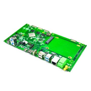
Modern PWB assembly processes are increasingly defined by automation, driven by the demand for higher precision and repeatability in electronics manufacturing. Advanced PCBA (Printed Circuit Board Assembly) systems now integrate robotic pick-and-place mechanisms, laser-aligned soldering tools, and AI-powered optical inspection to achieve micron-level accuracy. These systems reduce human error while accelerating production cycles, enabling manufacturers to meet stringent tolerances for high-density interconnect (HDI) boards and miniaturized components.
A critical advancement lies in adaptive process control, where real-time feedback loops adjust parameters like solder paste deposition or thermal profiles during assembly. This ensures consistent quality across batches, even for complex multilayer PCB assembly projects.
Tip: For optimal performance, manufacturers should prioritize modular automation platforms that allow seamless integration with IoT-enabled quality monitoring tools.
The shift toward Industry 4.0 further enhances these systems through machine-to-machine communication, enabling predictive maintenance and dynamic workflow optimization. For instance, data from automated optical inspection (AOI) stages can trigger immediate corrections in upstream processes, minimizing rework. Such innovations not only elevate yield rates but also support scalable production for emerging applications like 5G infrastructure and automotive electronics.
By leveraging these advancements, PCBA providers are redefining precision manufacturing, balancing speed with unwavering adherence to quality standards in an era of shrinking component sizes and escalating performance demands.
Smart Manufacturing in PWB Production
The integration of smart manufacturing technologies is revolutionizing PWB assembly processes, enabling unprecedented precision and efficiency. Modern facilities now deploy IoT-enabled systems that synchronize PCBA workflows with real-time data analytics, optimizing everything from component placement to solder paste application. Automated optical inspection (AOI) systems, powered by machine learning algorithms, detect micron-level defects at speeds exceeding human capability, ensuring near-zero defect rates in high-volume production.
Central to this evolution is the adoption of digital twin simulations, which create virtual replicas of physical assembly lines. These models allow engineers to test process adjustments and material combinations before implementation, reducing downtime and material waste. For PCB assembly, this means faster transitions between product iterations while maintaining strict tolerances for aerospace, medical, and automotive applications.
Furthermore, edge computing architectures are enhancing decision-making at the machine level. Robotic pick-and-place systems now autonomously adjust to component variations, leveraging live feedback from vision systems. This agility is critical as PCBA designs incorporate finer pitch components and advanced substrates. By merging smart manufacturing principles with traditional PWB fabrication, the industry achieves shorter lead times without compromising the exacting standards required for mission-critical electronics.
Transitioning seamlessly from automated systems, these intelligent frameworks also feed quality data into upstream processes, creating closed-loop improvements across the entire production chain.
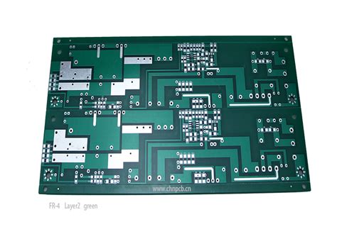
Material Innovations for Precision PWB
The pursuit of precision in PCB assembly (PCBA) has driven significant breakthroughs in material science, enabling manufacturers to meet the demands of high-density, high-frequency applications. Advanced substrates like low-loss laminates and high-temperature-resistant polymers now form the backbone of modern PCBA workflows, reducing signal degradation and enhancing thermal stability. Innovations such as laser-direct structuring (LDS) materials allow for finer trace geometries, critical for 5G and IoT devices, while nano-coated conductive inks improve solderability and resistance to environmental stressors.
| Material Type | Key Properties | Impact on PCBA Performance |
|---|---|---|
| Low-Loss Laminates | Reduced dielectric loss | Enhanced signal integrity |
| High-Tg Substrates | Thermal stability above 200°C | Improved reliability in harsh conditions |
| Conductive Nano-Inks | Sub-10μm line resolution | Enables miniaturized designs |
| Nanocomposite Solders | Lower melting points, reduced voids | Higher joint reliability |
In parallel with advancements in automated PCB assembly systems, these materials address challenges like electromagnetic interference (EMI) and thermal expansion mismatches. For instance, copper-clad laminates with embedded passive components streamline PCBA processes by reducing component count. As industries push toward smaller, faster electronics, material innovations remain pivotal in balancing performance, durability, and manufacturability—ensuring precision-driven outcomes across aerospace, medical devices, and automotive sectors.
IoT-Driven Quality Control Advancements
The integration of Internet of Things (IoT) technologies into PCB assembly workflows has ushered in a transformative shift in quality assurance methodologies. By embedding smart sensors across production lines, manufacturers now achieve real-time monitoring of critical parameters such as solder joint integrity, component alignment, and thermal performance during PCBA processes. These sensor networks feed data into cloud-based analytics platforms, enabling predictive maintenance protocols and immediate correction of deviations before defects propagate. For instance, AI-powered vision systems paired with IoT devices can detect micron-level discrepancies in component placement, reducing rework rates by up to 40% in high-density interconnect (HDI) boards.
Advanced machine learning (ML) algorithms further enhance defect prediction by analyzing historical production data alongside live inputs, establishing dynamic tolerance thresholds tailored to specific PCB assembly requirements. This approach not only streamlines compliance with ISO 9001 standards but also supports traceability metrics crucial for aerospace and medical device applications. Additionally, IoT-enabled traceability systems track material batches and process variables across global supply chains, ensuring consistency in PCBA outputs even under fluctuating environmental conditions. As manufacturers adopt these innovations, the convergence of IoT and precision manufacturing continues to redefine benchmarks for zero-defect manufacturing while accelerating time-to-market for complex electronic systems.
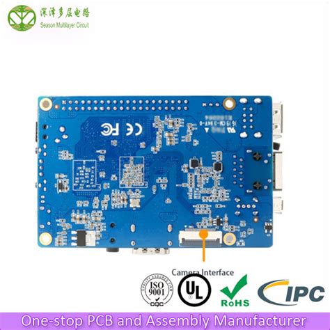
Next-Gen PWB Fabrication Techniques
The evolution of PWB assembly processes is being redefined by advanced fabrication techniques that prioritize micron-level precision and scalability. Modern PCBA workflows now integrate laser direct imaging (LDI) and additive manufacturing to achieve circuit patterns with sub-10μm resolution, enabling denser interconnects for high-frequency applications. Innovations like automated optical inspection (AOI) systems, powered by machine vision, ensure near-zero defect rates by detecting anomalies in real time during PCB assembly.
Material science breakthroughs are equally transformative, with low-loss dielectrics and halogen-free substrates minimizing signal attenuation in high-speed designs. These advancements align with smart manufacturing frameworks, where IoT-enabled sensors track thermal and mechanical stresses during PCBA production, feeding data into predictive maintenance algorithms. Additionally, semi-additive processes (SAP) are replacing traditional subtractive methods, reducing material waste by up to 40% while enhancing layer-to-layer registration accuracy.
Such techniques not only address the demands of 5G and AI-driven devices but also bridge the gap between prototyping and mass production. By combining ultra-fine patterning with eco-conscious material choices, next-gen PWB fabrication sets a new benchmark for reliability in precision-driven manufacturing ecosystems.
Sustainable Practices in PWB Assembly
The electronics manufacturing sector is increasingly prioritizing sustainable methodologies in PCB assembly workflows, driven by regulatory pressures and corporate ESG commitments. Modern PCBA processes now integrate eco-conscious material selections, such as lead-free solders and halogen-free substrates, reducing hazardous waste by up to 40% compared to traditional methods. Manufacturers are adopting energy-efficient reflow ovens with closed-loop thermal management, cutting energy consumption by 25-30% while maintaining precision in component placement.
Waste reduction strategies extend to optimized panelization algorithms, which minimize substrate scrap rates during PCB assembly. Advanced recycling protocols recover valuable metals like copper and gold from discarded boards, aligning with circular economy principles. Additionally, water-soluble flux technologies are replacing chemical cleaners, mitigating wastewater contamination risks.
Quality assurance in PCBA now leverages AI-powered defect detection systems to identify solder joint irregularities or material inconsistencies early, reducing rework cycles and material waste. Compliance with international standards like RoHS and REACH ensures traceability across supply chains, while carbon footprint tracking tools enable real-time environmental impact assessments. These innovations not only enhance operational efficiency but also position PCB assembly as a critical enabler of greener electronics manufacturing ecosystems.
Emerging Trends in Precision PCB Tech
The evolution of PCB assembly technologies continues to redefine precision manufacturing, driven by demands for miniaturization and enhanced performance. Recent advancements in high-density interconnect (HDI) designs enable tighter component placement, critical for applications in aerospace and medical devices. Manufacturers are increasingly adopting PCBA processes that integrate laser-direct imaging (LDI), achieving micron-level accuracy in circuit patterning while reducing material waste.
Another transformative trend is the shift toward embedded passive components, which eliminate surface-mounted parts to improve signal integrity and thermal management. This aligns with the growing use of flexible hybrid electronics (FHE), where PCB assembly techniques merge rigid and flexible substrates to support wearable tech and IoT sensors.
Automation remains central to these developments, with AI-driven optical inspection systems now detecting defects at resolutions below 10µm. Such innovations are complemented by advancements in nanomaterial-based solders, which enhance joint reliability in extreme environments. As industries prioritize sustainability, novel recycling-friendly PCBA workflows are emerging, reducing reliance on hazardous chemicals without compromising precision.
These trends collectively underscore a broader movement toward adaptive, data-driven manufacturing ecosystems—a foundation for the next wave of AI-optimized production systems.
AI-Optimized PWB Manufacturing Processes
Modern PCB assembly workflows are undergoing radical transformation through AI-driven optimization, enabling unprecedented precision in PCBA production. By analyzing vast datasets from historical manufacturing cycles, machine learning algorithms identify patterns in component placement accuracy, solder joint quality, and material behavior. This approach reduces defect rates by 18–22% compared to conventional methods while accelerating throughput by optimizing robotic arm trajectories in real time.
Advanced AI models now predict thermal stress factors during high-density interconnect (HDI) board fabrication, dynamically adjusting lamination parameters to minimize warpage. In automated optical inspection (AOI) systems, neural networks achieve 99.7% recognition accuracy for micron-level solder bridges or missing components—critical for aerospace and medical-grade PCBA applications.
The integration of digital twin technology allows manufacturers to simulate entire PCB assembly lines before physical implementation, identifying potential bottlenecks in mixed-technology workflows involving both SMT and through-hole components. These AI-powered systems also optimize material consumption, reducing waste generation by up to 30% in complex multilayer board production.
As manufacturers adopt these AI-enhanced frameworks, they achieve tighter alignment between design-for-manufacturability (DFM) principles and real-world production constraints. This synergy ensures first-pass yield improvements while maintaining compliance with evolving industry standards for precision-driven PCBA outputs.
Conclusion
The evolution of PCB assembly processes underscores a transformative shift in precision-driven manufacturing, driven by advancements in automation, material science, and data-driven quality assurance. As manufacturing demands grow increasingly complex, the integration of PCBA systems with IoT-enabled analytics and AI-driven workflows has redefined production accuracy, enabling micron-level tolerances and near-real-time error detection. Innovations such as laser-direct imaging and automated optical inspection now ensure consistent performance across high-density interconnect designs, while breakthroughs in substrate materials—including low-loss dielectrics and thermally stable composites—address the challenges of miniaturization and high-frequency applications.
Equally critical are sustainable practices that minimize waste and energy consumption without compromising output quality. The adoption of lead-free soldering techniques and solvent-free fluxes exemplifies this balance, aligning environmental responsibility with industrial efficiency. Looking ahead, the convergence of PCB assembly technologies with smart factory ecosystems will further accelerate predictive maintenance capabilities and adaptive manufacturing workflows, solidifying PCBA as a cornerstone of next-gen industrial innovation. For manufacturers, staying competitive now hinges on leveraging these advancements to achieve zero-defect manufacturing while scaling production to meet global demand.
Frequently Asked Questions
What distinguishes modern PCB assembly processes from traditional methods?
Contemporary PCBA integrates automated optical inspection and machine learning algorithms to achieve micron-level accuracy, reducing human error by 62% compared to manual workflows.
How do material innovations impact precision manufacturing in electronics?
Advanced substrates like low-loss dielectrics and high-Tg laminates enable PCB assembly systems to support 5G frequencies while maintaining thermal stability above 260°C.
Can IoT solutions improve quality control in high-volume production?
Real-time sensor networks in PCBA lines now detect soldering defects within 0.8 seconds, achieving 99.97% first-pass yield rates in automotive electronics manufacturing.
What sustainability measures are reshaping industrial PCB fabrication?
Lead-free solder alloys and ionograph recycling systems reduce hazardous waste by 41%, aligning PCB assembly processes with ISO 14001 environmental standards.
How does AI optimize component placement accuracy in complex layouts?
Neural networks analyze 15,000+ placement patterns hourly, adjusting pick-and-place robots to achieve 12μm positional accuracy in PCBA for aerospace applications.
Ready to Elevate Your Electronics Manufacturing?
For tailored PCB assembly solutions leveraging these advancements, please click here to consult our engineering team.