Quality Control in PCB Manufacturing: Ensuring Design Specifications Are Met
Introduction
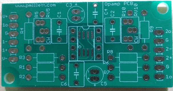
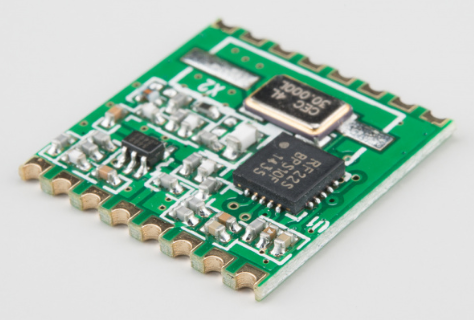
Printed Circuit Boards (PCBs) are the backbone of modern electronics, forming the foundation of devices ranging from smartphones to industrial machinery. Ensuring that PCBs meet design and manufacturing specifications is crucial for functionality, reliability, and performance. Manufacturers employ rigorous inspection and testing procedures to verify that each PCB adheres to the required standards before shipment.
This article explores the key quality control (QC) processes used in PCB manufacturing to confirm that the final product meets design and process requirements. These methods include visual inspections, automated optical inspections (AOI), electrical testing, and other advanced techniques.
1. Visual Inspection
1.1 Manual Visual Inspection (MVI)
Manual visual inspection is the most basic yet essential step in PCB quality control. Skilled technicians examine PCBs for visible defects such as:
- Solder bridges (unintended connections between pads)
- Insufficient or excessive solder
- Misaligned components
- Scratches or physical damage
- Incorrectly placed or missing components
While MVI is cost-effective, it is prone to human error, especially in high-volume production.
1.2 Automated Optical Inspection (AOI)
AOI systems use high-resolution cameras and image-processing software to detect defects more accurately than manual inspection. Key advantages include:
- Higher speed and consistency
- Detection of microscopic flaws (e.g., tiny cracks, incorrect solder paste application)
- Comparison against design files to verify component placement
AOI is typically used after solder paste application, post-reflow, and before final electrical testing.
2. Electrical Testing
2.1 Continuity Testing (Short-Circuit Check)
A continuity test ensures that no unintended connections (shorts) exist between traces. This is done using a multimeter or automated test equipment (ATE) that checks resistance between conductive paths.
2.2 Insulation Resistance Testing
This test verifies that insulating materials (e.g., solder mask, substrate) prevent leakage currents between conductors. High-voltage tests (typically 100V–500V) are applied to ensure no breakdown occurs.
2.3 Flying Probe Testing
Flying probe testers use movable probes to check electrical connectivity without requiring a custom test fixture. They are ideal for prototypes and low-volume production, checking:
- Open circuits (broken traces)
- Short circuits
- Component values (resistance, capacitance, etc.)
2.4 In-Circuit Testing (ICT)
ICT is a more comprehensive electrical test for high-volume production. A bed-of-nails fixture makes contact with test points on the PCB to verify:
- Correct component values (resistors, capacitors, etc.)
- Proper soldering of integrated circuits (ICs)
- Signal integrity in critical paths
ICT is highly accurate but requires custom fixtures, making it cost-effective only for large production runs.
3. Functional Testing
Functional testing ensures the PCB operates as intended in its final application. This involves:
- Powering up the board and running firmware/software tests
- Checking signal integrity (e.g., high-speed digital or RF circuits)
- Verifying input/output responses (e.g., sensor readings, communication protocols)
Functional testing may include boundary scan (JTAG) for complex digital circuits, where embedded test structures validate interconnections.
4. X-Ray Inspection (AXI)
Automated X-ray inspection (AXI) is critical for detecting hidden defects, especially in:
- Ball Grid Array (BGA) and Quad Flat No-Lead (QFN) packages (where solder joints are not visible)
- Multilayer PCBs (internal trace integrity)
- Voids or cracks in solder joints
AXI provides 2D or 3D imaging, allowing manufacturers to assess solder quality without destructive testing.
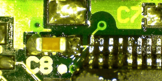
5. Microsectioning (Cross-Sectional Analysis)
For critical applications (e.g., aerospace, medical devices), manufacturers perform destructive testing by cutting a PCB sample and examining its internal structure under a microscope. This helps verify:
- Plated through-hole (PTH) quality
- Layer alignment in multilayer PCBs
- Solder joint integrity
While destructive, microsectioning provides definitive evidence of manufacturing quality.
6. Environmental and Reliability Testing
To ensure long-term reliability, PCBs undergo stress tests simulating real-world conditions:
- Thermal cycling (exposing the PCB to extreme temperature changes to detect delamination or solder cracks)
- Humidity testing (evaluating resistance to moisture absorption)
- Vibration and shock testing (for automotive/military applications)
- High-voltage stress testing (HVS) (for insulation breakdown risks)
These tests help identify potential failure modes before the PCB reaches the end user.
7. Compliance with Industry Standards
PCB manufacturers must adhere to industry standards such as:
- IPC-A-600 (Acceptability of Printed Boards)
- IPC-6012 (Qualification and Performance Specification for Rigid PCBs)
- ISO 9001 (Quality Management Systems)
- UL certification (for safety compliance)
Compliance ensures consistency and reliability across production batches
Conclusion
Ensuring that PCBs meet design and manufacturing requirements involves a combination of visual inspections, electrical tests, functional validation, and reliability assessments. Advanced techniques like AOI, AXI, and ICT enhance defect detection, while environmental testing guarantees long-term performance.
By implementing these rigorous QC measures, manufacturers can deliver high-quality PCBs that meet industry standards and customer expectations, reducing field failures and ensuring optimal performance in electronic devices.


