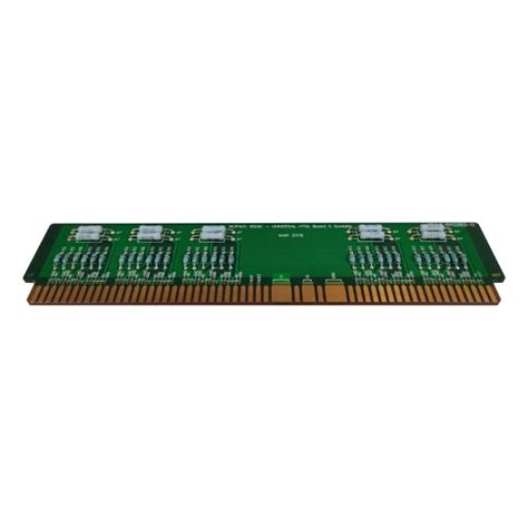
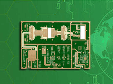
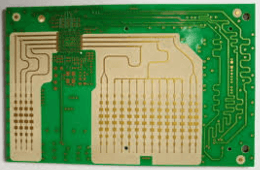
Quick turn heavy copper pcb
Benefits Of Quick Turn Heavy Copper PCB In High-Power Applications
Quick turn heavy copper PCBs have become increasingly significant in high-power applications, offering a multitude of benefits that enhance performance, reliability, and efficiency. These specialized printed circuit boards are designed with thicker copper layers, typically ranging from 3 to 20 ounces per square foot, which enable them to handle higher currents and dissipate heat more effectively than standard PCBs. The rapid turnaround time associated with quick turn heavy copper PCBs further amplifies their advantages, making them an ideal choice for industries that demand both high power and swift production cycles.
One of the primary benefits of quick turn heavy copper PCBs in high-power applications is their superior current-carrying capacity.
The increased thickness of the copper layers allows these PCBs to conduct higher currents without experiencing excessive heat buildup. This is particularly crucial in applications such as power supplies, automotive electronics, and industrial control systems, where efficient power management is essential. By accommodating higher currents, heavy copper PCBs reduce the risk of overheating and potential failure, thereby enhancing the overall reliability and longevity of the electronic devices they support.
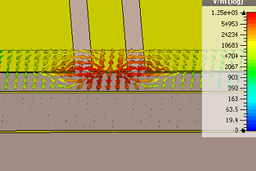
In addition to their enhanced current-carrying capacity, heavy copper PCBs offer improved thermal management.
The thicker copper layers act as effective heat sinks, dissipating heat more efficiently and preventing hotspots that could damage sensitive components. This thermal efficiency is vital in high-power applications where excessive heat can compromise performance and lead to system failures. By maintaining optimal operating temperatures, heavy copper PCBs ensure that electronic devices function reliably even under demanding conditions.
Moreover, the mechanical strength of heavy copper PCBs is another significant advantage.
The robust construction of these PCBs makes them more resistant to mechanical stresses, such as bending and vibration, which are common in high-power applications. This durability is particularly beneficial in environments where electronic devices are subjected to harsh conditions, such as in aerospace, military, and industrial settings. The enhanced mechanical strength of heavy copper PCBs contributes to their overall reliability and reduces the likelihood of damage during operation.
The quick turn aspect of these PCBs further enhances their appeal in high-power applications.
Rapid production and delivery times are critical in industries where time-to-market is a key competitive factor. Quick turn heavy copper PCBs enable manufacturers to meet tight deadlines and respond swiftly to market demands. This agility is especially important in sectors such as consumer electronics and telecommunications, where technological advancements and market trends evolve rapidly. By minimizing lead times, quick turn heavy copper PCBs help companies stay ahead of the competition and bring innovative products to market faster.
Furthermore, the design flexibility offered by heavy copper PCBs is a notable benefit.
The ability to incorporate multiple copper layers and complex circuit designs allows engineers to create more efficient and compact solutions for high-power applications. This flexibility is essential in optimizing the performance and functionality of electronic devices, enabling the integration of advanced features and capabilities. As a result, heavy copper PCBs facilitate the development of cutting-edge technologies that meet the evolving needs of various industries.
In conclusion, quick turn heavy copper PCBs provide a range of benefits that make them indispensable in high-power applications. Their superior current-carrying capacity, improved thermal management, mechanical strength, rapid production times, and design flexibility collectively enhance the performance, reliability, and efficiency of electronic devices. As industries continue to demand more powerful and efficient solutions, the importance of quick turn heavy copper PCBs in high-power applications is likely to grow, driving further innovation and advancement in the field of electronics.
Design Considerations For Quick Turn Heavy Copper PCB
When designing a quick turn heavy copper PCB, several critical considerations must be taken into account to ensure optimal performance and reliability. Heavy copper PCBs, characterized by their thick copper layers, are essential in applications requiring high current carrying capacity and enhanced thermal management. The design process for these specialized PCBs involves meticulous planning and a deep understanding of the unique challenges they present.
One of the primary considerations in designing heavy copper PCBs is the selection of appropriate materials.
The substrate material must be capable of withstanding the high temperatures associated with the increased current loads. FR-4, a commonly used substrate, may not always be suitable for heavy copper applications due to its thermal limitations. Therefore, alternative materials such as polyimide or ceramic substrates might be considered to ensure the board’s integrity under extreme conditions.
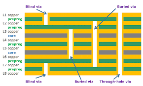
Another crucial aspect is the copper thickness itself.
Standard PCBs typically use copper layers ranging from 1 to 3 ounces per square foot, whereas heavy copper PCBs can have copper layers exceeding 20 ounces per square foot. This significant increase in copper thickness necessitates adjustments in the PCB manufacturing process, including specialized etching techniques and extended plating times. These adjustments ensure that the copper layers are uniformly distributed and adhere properly to the substrate, preventing issues such as delamination or uneven current distribution.
Thermal management is another vital factor in the design of heavy copper PCBs.
The increased copper thickness enhances the board’s ability to dissipate heat, which is beneficial for high-power applications. However, this also means that designers must carefully consider the placement of components and the overall layout to optimize heat dissipation. Thermal vias, heat sinks, and other cooling mechanisms may be incorporated into the design to manage the heat effectively and prevent hotspots that could damage components or reduce the board’s lifespan.
Electrical considerations are equally important when designing heavy copper PCBs.
The increased copper thickness allows for higher current carrying capacity, which is advantageous for power electronics and other high-current applications. However, this also means that trace widths and spacing must be carefully calculated to handle the increased current without causing excessive heat buildup or electrical interference. Advanced simulation tools can be employed to model the electrical behavior of the PCB and ensure that the design meets the required specifications.
Moreover, the mechanical properties of the PCB must be taken into account.
Heavy copper PCBs are inherently more robust and durable than their standard counterparts, making them suitable for harsh environments and applications requiring high mechanical strength. However, this also means that the board may be less flexible, which could pose challenges during assembly and installation. Designers must consider these mechanical constraints and ensure that the PCB can be integrated seamlessly into the final product without compromising its structural integrity.
In addition to these technical considerations, the quick turn aspect of heavy copper PCB design introduces its own set of challenges.
Rapid prototyping and production require efficient communication between the design team and the manufacturer. Detailed documentation, including precise specifications and clear design files, is essential to minimize errors and ensure a smooth production process. Collaboration with experienced manufacturers who specialize in heavy copper PCBs can significantly reduce lead times and improve the overall quality of the final product.
In conclusion, designing a quick turn heavy copper PCB involves a comprehensive understanding of material selection, thermal management, electrical considerations, mechanical properties, and efficient communication with manufacturers. By addressing these factors meticulously, designers can create robust, high-performance PCBs that meet the demanding requirements of modern electronic applications.
Manufacturing Process Of Quick Turn Heavy Copper PCB
The manufacturing process of quick turn heavy copper PCBs is a sophisticated and intricate procedure that demands precision and expertise. This type of printed circuit board (PCB) is characterized by its thick copper layers, which can range from 3 oz/ft² to 20 oz/ft² or more. These heavy copper layers are essential for applications requiring high current carrying capacity and enhanced thermal management. To achieve a quick turnaround, manufacturers must streamline each step of the process while maintaining stringent quality standards.
Initially, the process begins with the selection of high-quality raw materials.
The base material, typically a copper-clad laminate, is chosen based on the specific requirements of the PCB design. The laminate is then cleaned and prepared for the subsequent steps. Following this, the design layout is transferred onto the laminate using a process called photoresist imaging. This involves coating the laminate with a light-sensitive material and exposing it to ultraviolet light through a photomask, which contains the desired circuit pattern. The exposed areas of the photoresist harden, while the unexposed areas remain soft and are subsequently removed, revealing the underlying copper.
Next, the PCB undergoes an etching process to remove the unwanted copper.
This is achieved by immersing the board in a chemical solution that dissolves the exposed copper, leaving behind the desired circuit pattern. For heavy copper PCBs, this step requires careful control to ensure that the thick copper layers are etched uniformly without compromising the integrity of the circuit traces. Once the etching is complete, the remaining photoresist is stripped away, and the board is thoroughly cleaned.
Following the etching process, the PCB is subjected to a series of plating steps to build up the copper thickness.
Electroplating is commonly used for this purpose, where the board is immersed in an electrolytic solution and an electric current is applied. This causes copper ions to deposit onto the exposed copper surfaces, gradually increasing the thickness of the copper layers. For heavy copper PCBs, multiple plating cycles may be necessary to achieve the desired thickness. Throughout this process, precise control of the plating parameters is crucial to ensure uniform copper deposition and to prevent defects such as voids or uneven surfaces.
After the copper plating is complete, the PCB undergoes a series of additional processes to prepare it for final assembly.
These include drilling holes for vias and mounting components, applying a solder mask to protect the circuit traces, and printing the silkscreen layer for component identification. Each of these steps requires meticulous attention to detail to ensure that the final product meets the required specifications.
Finally, the PCB is subjected to rigorous testing and inspection to verify its functionality and quality.
Electrical tests are conducted to check for continuity and to ensure that there are no short circuits or open circuits. Additionally, visual inspections and automated optical inspections (AOI) are performed to detect any physical defects. Once the PCB passes all tests, it is ready for shipment to the customer.
In conclusion, the manufacturing process of quick turn heavy copper PCBs involves a series of carefully controlled steps, from material selection and imaging to etching, plating, and final testing. Each stage requires precision and expertise to ensure that the final product meets the high standards required for demanding applications. By streamlining these processes and maintaining rigorous quality control, manufacturers can achieve quick turnaround times while delivering reliable and high-performance PCBs.
Cost-Effective Solutions For Quick Turn Heavy Copper PCB Production
In the realm of modern electronics, the demand for quick turn heavy copper PCBs has surged, driven by the need for robust and reliable circuit boards capable of handling high current loads and thermal management challenges. Heavy copper PCBs, characterized by their thick copper layers, are essential in applications such as power supplies, automotive electronics, and industrial controls. However, the production of these specialized PCBs can be cost-intensive, necessitating innovative approaches to ensure cost-effectiveness without compromising quality or performance.
One of the primary strategies to achieve cost-effective quick turn heavy copper PCB production is the optimization of the manufacturing process.
By streamlining production workflows and employing advanced fabrication techniques, manufacturers can significantly reduce lead times and costs. For instance, the use of direct imaging technology in the photolithography process enhances precision and reduces material wastage, thereby lowering production expenses. Additionally, implementing automated inspection systems ensures high-quality standards are maintained while minimizing manual labor costs.
Moreover, material selection plays a crucial role in the cost-efficiency of heavy copper PCBs.
While the use of thick copper layers is indispensable for these PCBs, manufacturers can explore alternative materials for other layers to balance performance and cost. For example, using high-temperature laminates and substrates that offer excellent thermal conductivity can enhance the PCB’s durability and reliability, potentially reducing the need for additional cooling mechanisms. This approach not only cuts down on material costs but also simplifies the overall design, leading to faster production cycles.
Furthermore, leveraging economies of scale can be a significant factor in reducing costs.
By consolidating orders and producing heavy copper PCBs in larger batches, manufacturers can benefit from bulk purchasing of raw materials and more efficient use of production resources. This strategy is particularly effective for industries with consistent demand for heavy copper PCBs, as it allows for better planning and resource allocation. Additionally, collaborating with suppliers to negotiate favorable terms and prices for bulk orders can further enhance cost savings.
Another critical aspect of cost-effective quick turn heavy copper PCB production is the adoption of design for manufacturability (DFM) principles.
By incorporating DFM guidelines during the design phase, engineers can create PCB layouts that are easier and more cost-effective to produce. This includes optimizing trace widths and spacing, minimizing the number of layers, and ensuring that the design adheres to standard manufacturing capabilities. DFM not only reduces the likelihood of production errors but also shortens the time required for prototyping and testing, ultimately accelerating the time-to-market.
In addition to these strategies, investing in advanced manufacturing equipment and technologies can yield long-term cost benefits.
Modern equipment, such as laser drilling machines and high-precision etching tools, can enhance production efficiency and accuracy, reducing the need for rework and scrap. While the initial investment may be substantial, the long-term savings in production costs and improved product quality can justify the expenditure.
Lastly, fostering a culture of continuous improvement within the manufacturing organization is essential for maintaining cost-effectiveness. Regularly reviewing and refining production processes, staying abreast of technological advancements, and training staff on best practices can lead to incremental improvements that collectively result in significant cost savings. By embracing a proactive approach to process optimization and innovation, manufacturers can remain competitive in the fast-paced electronics industry.
In conclusion, achieving cost-effective solutions for quick turn heavy copper PCB production requires a multifaceted approach that encompasses process optimization, strategic material selection, economies of scale, DFM principles, advanced manufacturing technologies, and a commitment to continuous improvement. By integrating these elements, manufacturers can deliver high-quality heavy copper PCBs efficiently and economically, meeting the growing demands of various high-performance applications.