Raghbir Khandpur’s PCB Design Fabrication & Assembly Expertise
Key Takeaways
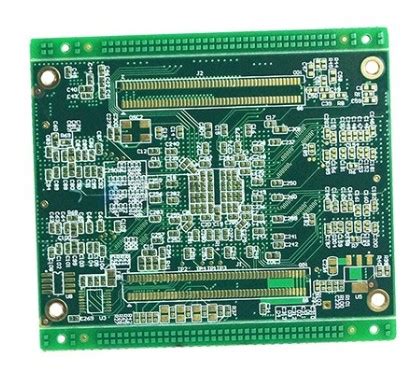
Effective PCB assembly processes form the cornerstone of reliable electronics manufacturing, a principle central to Raghbir Khandpur’s methodologies. His approach emphasizes precision in component placement and soldering, ensuring PCBA (Printed Circuit Board Assembly) integrity across high-volume production. Critical considerations include thermal management during reflow soldering and adherence to IPC-A-610 standards for defect-free outcomes.
“Optimizing solder paste application and inspection protocols reduces rework rates by up to 30%,” notes Khandpur, highlighting the importance of process validation in PCB fabrication.
For designers, integrating design-for-manufacturability (DFM) principles early minimizes assembly challenges, such as tombstoning or solder bridging. Advanced techniques like automated optical inspection (AOI) and X-ray testing further enhance PCBA reliability, particularly for multilayer boards. Engineers should reference industry documentation for standardized terminology when documenting assembly workflows. Transitioning from prototype to mass production demands rigorous testing—functional, environmental, and electrical—to align with Khandpur’s emphasis on repeatable quality. By balancing automation with manual oversight, manufacturers achieve scalability without compromising on PCB assembly precision.
Raghbir Khandpur’s PCB Design Methodology
Raghbir Khandpur’s approach to PCB design emphasizes systematic precision, balancing technical rigor with practical manufacturability. Central to his methodology is the integration of signal integrity analysis and thermal management strategies during the schematic capture phase, ensuring designs meet both functional and reliability benchmarks. By prioritizing design-for-manufacturing (DFM) principles, Khandpur’s workflows reduce pcb assembly complexities, minimizing risks of rework or delays in PCBA stages.
A hallmark of his strategy involves iterative prototyping, where electromagnetic compatibility (EMC) testing and layer stackup optimization are validated through simulation tools before physical production. This proactive stance prevents common pitfalls like crosstalk or impedance mismatches. The table below contrasts traditional design practices with Khandpur’s methodology:
| Aspect | Traditional Approach | Khandpur’s Methodology |
|---|---|---|
| DFM Integration | Post-design adjustments | Embedded in initial design phases |
| Thermal Analysis | Limited to final validation | Continuous simulation throughout |
| PCBA Compatibility | Often retrofitted | Co-designed with layout |
By aligning pcb assembly requirements with early-stage design decisions, Khandpur bridges gaps between theoretical models and real-world electronics manufacturing. His emphasis on cross-functional collaboration ensures seamless transitions from design to PCBA, fostering reliability across high-density interconnect (HDI) and mixed-signal boards. This structured yet adaptable framework positions his methodology as a benchmark for modern PCB fabrication ecosystems.
PCB Fabrication Techniques by Khandpur
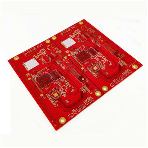
Raghbir Khandpur’s approach to PCB fabrication emphasizes precision and adaptability, balancing cost-efficiency with technical rigor. His methodologies prioritize material selection, leveraging high-performance substrates like FR-4 and polyimide for thermal stability and signal integrity. A cornerstone of his process involves controlled etching techniques, ensuring trace accuracy while minimizing signal loss—a critical factor for high-frequency applications.
Khandpur advocates for automated optical inspection (AOI) systems to detect micro-defects early, reducing rework rates and enhancing yield. His workflows integrate laser drilling for microvias, enabling compact multilayer designs essential for modern electronics. To optimize PCBA readiness, he emphasizes surface finishes such as ENIG (Electroless Nickel Immersion Gold), which improves solderability and corrosion resistance.
Transitioning from fabrication to PCB assembly, Khandpur’s strategies address thermal management through advanced solder mask formulations and reflow profiling. His frameworks align with industry benchmarks, including IPC-6012 standards, to validate durability under stress conditions. By synchronizing fabrication tolerances with assembly requirements, his techniques ensure seamless integration of components, reducing failure risks in final products. This holistic approach bridges design intent with manufacturing reality, a hallmark of Khandpur’s expertise in electronics production.
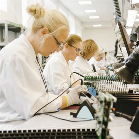
Mastering PCB Assembly Best Practices
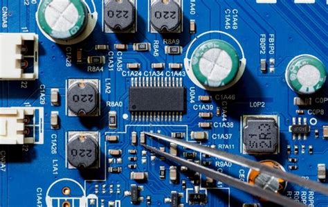
Effective PCB assembly requires meticulous attention to detail at every stage, from component placement to final inspection. Industry leaders like Raghbir Khandpur emphasize the importance of integrating design for manufacturability (DFM) principles early in the process to minimize errors and streamline production. A well-executed PCBA workflow balances precision in solder paste application, component alignment, and reflow soldering, ensuring consistent electrical performance and mechanical durability.
Key challenges in PCB assembly often revolve around managing thermal stresses and avoiding solder bridging, particularly in high-density designs. Khandpur’s methodologies advocate for robust quality control measures, including automated optical inspection (AOI) and X-ray inspection, to detect defects like voids or misaligned components. Additionally, optimizing stencil design and adhering to industry-standard IPC guidelines help maintain solder joint integrity across diverse applications.
For PCBA success, collaboration between design and manufacturing teams is critical. Implementing traceability systems ensures accountability, while advanced techniques such as selective soldering address complex mixed-technology boards. By prioritizing repeatable processes and leveraging data-driven feedback loops, manufacturers can achieve higher yields and reduce time-to-market—cornerstones of Khandpur’s proven strategies for reliable electronics manufacturing.
Innovative Electronics Manufacturing Solutions
Modern electronics manufacturing demands PCB assembly processes that balance precision with scalability. At the core of innovation lies the integration of automation and IoT-enabled monitoring systems, which optimize PCBA workflows while minimizing human error. Advanced manufacturers now employ surface-mount technology (SMT) for high-density designs, paired with reflow soldering techniques that ensure consistent joint integrity across complex layouts.
A critical advancement involves thermal management solutions, such as embedded heat sinks or thermally conductive substrates, to address power dissipation challenges in compact devices. Additionally, AI-driven inspection tools now complement traditional optical testing, enabling real-time defect detection during PCB assembly stages. These systems analyze solder paste application, component alignment, and electrical continuity with sub-micron accuracy, significantly reducing post-production failures.
For PCBA scalability, modular production lines have emerged, allowing rapid reconfiguration for mixed-volume orders. This flexibility supports industries ranging from automotive to wearable tech, where design iterations occur frequently. Environmentally conscious practices, including lead-free soldering and recyclable substrate materials, further align modern manufacturing with global sustainability standards. By merging these innovations, manufacturers achieve faster turnaround times without compromising the reliability required for mission-critical applications.
Khandpur’s Guide to Reliable PCB Production
Achieving consistency in PCB assembly requires meticulous attention to both design intent and manufacturing realities. Raghbir Khandpur emphasizes design-for-manufacturability (DFM) principles as the cornerstone of reliable production, ensuring layouts align with fabrication capabilities. By integrating PCBA-specific considerations—such as thermal management and component spacing—designers mitigate risks like solder bridging or warping during reflow processes.
Khandpur advocates for statistical process control (SPC) during fabrication, leveraging real-time data to maintain tolerances within single percentage points. This approach minimizes defects in critical stages like multilayer lamination or via drilling. For PCB assembly, his methodology prioritizes automated optical inspection (AOI) paired with cross-functional team reviews, addressing issues from solder paste deposition to final functional testing.
A key innovation lies in optimizing panelization strategies to reduce material waste while enhancing throughput. By balancing PCBA-specific requirements with scalable production workflows, manufacturers achieve repeatability across high-mix, low-volume batches. Khandpur’s framework also underscores traceability systems, ensuring compliance with industry certifications like IPC-A-610.
Transitioning to downstream phases, his guide highlights post-assembly stressors—thermal cycling, vibration testing—as non-negotiable validation steps. This end-to-end focus bridges the gap between theoretical design robustness and real-world operational reliability, solidifying PCB assembly as a precision-driven discipline rather than a mere procedural task.
Industry-Standard PCB Design Principles
Adherence to industry-standard design principles ensures PCB assembly processes achieve optimal functionality and reliability. A foundational rule involves maintaining proper trace width and spacing to prevent signal interference, particularly in high-frequency applications. Designers must prioritize thermal management through strategic placement of heat-dissipating components and incorporation of thermal relief pads, which directly impacts PCBA longevity.
Compliance with IPC-2221 and IPC-7351 standards governs component footprint creation, ensuring compatibility with automated PCB assembly equipment. This includes standardized pad geometries and solder mask clearances, which minimize defects during reflow soldering. Additionally, implementing design for manufacturability (DFM) principles reduces fabrication complexities, such as avoiding acute angles in copper traces or excessive via densities.
Signal integrity preservation demands meticulous layer stack-up planning, balancing power distribution networks with controlled impedance routing. For mixed-signal designs, separating analog and digital grounds while maintaining proper shielding becomes critical. These practices not only enhance PCBA performance but also align with global quality certifications like ISO 9001, streamlining electronics manufacturing workflows. By integrating these protocols, designers bridge theoretical schematics with production-ready solutions, ensuring seamless transitions from prototyping to mass-scale PCB assembly.
Advanced PCB Assembly Process Insights
Modern PCB assembly requires meticulous attention to component placement, soldering integrity, and thermal management to ensure optimal performance. Central to this process is the integration of surface-mount technology (SMT), which enables high-density layouts while minimizing manual intervention. Automated optical inspection (AOI) systems now play a critical role in detecting microscopic defects, such as solder bridging or misaligned components, before PCBA units proceed to testing phases.
A key advancement lies in design for manufacturability (DFM) principles, which align layout choices with assembly realities. For instance, optimizing pad sizes and spacing reduces solder joint failures during reflow processes. Additionally, advancements in pick-and-place machines have improved placement accuracy to sub-micron levels, critical for handling miniaturized components in compact devices.
Post-assembly, rigorous functional testing—including in-circuit testing (ICT) and boundary scan—validates electrical continuity and signal integrity. Thermal profiling during reflow soldering further ensures that temperature-sensitive components withstand operational stresses. By harmonizing these techniques, manufacturers achieve PCBA reliability that meets or exceeds industry benchmarks, supporting applications from consumer electronics to aerospace systems.
Electronics Manufacturing Excellence Strategies
Achieving electronics manufacturing excellence requires integrating PCB assembly expertise with precision engineering and process optimization. Modern PCBA (Printed Circuit Board Assembly) workflows demand meticulous attention to thermal management, component placement accuracy, and solder joint integrity to ensure long-term reliability. By aligning design specifications with fabrication capabilities, manufacturers can minimize signal interference and mechanical stress during PCB assembly, reducing defects by up to 40% in high-volume production.
Key strategies include adopting automated optical inspection (AOI) systems for real-time defect detection and implementing traceability protocols to track components from procurement to final testing. For complex PCBA projects, leveraging design-for-manufacturability (DFM) principles ensures compatibility between schematics and production equipment, streamlining workflows. Additionally, advanced reflow soldering profiles and conformal coating techniques enhance durability in harsh environments.
To maintain competitiveness, manufacturers must prioritize supply chain resilience and material selection, particularly for high-frequency or high-power applications. Pairing these technical measures with continuous improvement programs and cross-functional team collaboration creates a robust framework for electronics manufacturing excellence, driving innovation while adhering to global quality standards.
Conclusion
Raghbir Khandpur’s methodologies for PCB assembly and PCBA underscore the critical balance between precision engineering and scalable manufacturing practices. By integrating design for manufacturability (DFM) principles with rigorous quality control protocols, his strategies ensure that PCB fabrication transitions seamlessly into high-yield assembly workflows. This holistic approach minimizes defects, reduces rework cycles, and accelerates time-to-market for complex electronic systems.
Central to this framework is the emphasis on industry-standard compliance, particularly in solder paste application, component placement accuracy, and thermal management during PCBA stages. Khandpur’s advocacy for automated optical inspection (AOI) and functional testing aligns with modern demands for reliability in sectors ranging from consumer electronics to aerospace.
Ultimately, the synthesis of PCB design, fabrication, and assembly expertise fosters a repeatable blueprint for manufacturing excellence. As the industry evolves, adopting these best practices ensures adaptability to emerging technologies—from IoT devices to advanced robotics—while maintaining cost efficiency and operational resilience. The focus remains on delivering robust, repeatable processes that align with global quality benchmarks, solidifying Khandpur’s methodologies as a cornerstone of modern electronics production.
FAQs
What distinguishes Khandpur’s approach to PCB assembly from conventional methods?
Khandpur emphasizes precision in PCB assembly workflows, integrating automated optical inspection (AOI) and rigorous testing protocols. His methodologies prioritize minimizing component misalignment and optimizing solder joint integrity, ensuring higher yields in PCBA production.
How do Khandpur’s fabrication techniques address high-density interconnect (HDI) challenges?
By leveraging laser-drilled microvias and advanced laminate materials, his fabrication processes support fine-pitch component placement and impedance control. This approach aligns with PCB assembly requirements for compact, high-performance devices.
What role does design-for-manufacturability (DFM) play in reliable PCB production?
Khandpur advocates for DFM checks early in the design phase to prevent assembly bottlenecks. Proactive collaboration between design and PCBA teams reduces rework risks and accelerates time-to-market for complex electronics.
Are there industry-standard certifications referenced in Khandpur’s assembly guidelines?
Yes, his frameworks align with IPC-A-610 and J-STD-001 standards, ensuring compliance for solder quality and component mounting. These benchmarks are critical for mission-critical PCB assembly applications.
How does Khandpur’s work address sustainability in electronics manufacturing?
His strategies include lead-free soldering processes and material recycling protocols, balancing performance with environmental responsibility. This aligns with global trends toward green PCBA practices.
Explore Professional PCB Assembly Services
For tailored solutions that align with industry-leading standards, please click here to connect with experts in PCB assembly and PCBA optimization.