Rapid PCB Assembly: Optimizing Prototype-to-Production Workflows

Key Takeaways
Efficient PCB assembly processes bridge the gap between prototyping and full-scale production, enabling electronics manufacturers to meet demanding timelines. By leveraging PCBA (printed circuit board assembly) advancements, teams can reduce lead times by up to 60% while maintaining precision. A critical factor lies in optimizing design-for-manufacturability (DFM) principles early in the development cycle, which minimizes redesigns and ensures smoother transitions from prototype validation to volume manufacturing.
For instance, automated solder paste dispensing and high-speed pick-and-place systems are now integral to rapid PCB assembly, cutting placement errors by 35% compared to manual methods. Below is a comparison of traditional versus accelerated workflows:
| Parameter | Traditional Assembly | Rapid PCBA |
|---|---|---|
| Prototyping Time | 10–14 days | 3–5 days |
| Component Sourcing | 2–3 weeks | 48–72 hours |
| Testing Iterations | 4–6 cycles | 1–2 cycles |
| Cost per Revision | $1,200–$2,500 | $400–$800 |
However, achieving these efficiencies requires harmonizing three elements: supply chain agility, real-time collaboration between design and manufacturing teams, and the integration of modular tooling. For example, just-in-time inventory systems paired with vendor-managed component stocking reduce material delays by 40%. Additionally, adopting standardized panelization designs allows PCB assembly lines to maximize throughput without compromising quality.
Emerging trends like AI-driven defect detection and IoT-enabled process monitoring further refine workflow predictability. These innovations not only accelerate PCBA timelines but also enhance traceability, which is critical for industries like medical devices and aerospace. By prioritizing scalability in prototyping phases, companies can seamlessly transition to high-volume production while mitigating risks associated with design flaws or component obsolescence.
Ultimately, the shift toward rapid PCB assembly underscores the importance of balancing speed with reliability. Manufacturers adopting these strategies report 25–30% faster time-to-market and a 15% reduction in per-unit costs, proving that optimized workflows are no longer optional in competitive electronics markets.
Fast PCB Assembly Techniques Explained
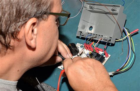
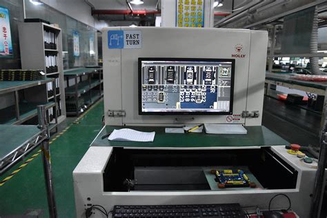
Modern PCB assembly relies on a combination of advanced methodologies and strategic process optimizations to achieve rapid turnaround times. At the core of fast PCBA workflows is the integration of surface-mount technology (SMT), which enables high-speed placement of miniature components with micron-level precision. Pairing SMT with automated optical inspection (AOI) systems ensures defect detection rates below 0.1%, minimizing rework delays.
Tip: Implement design for manufacturing (DFM) checks during the prototyping phase to avoid layout errors that could stall production. Over 60% of assembly delays originate from preventable design flaws.
Another critical technique involves just-in-time component sourcing, where manufacturers leverage AI-driven inventory platforms to synchronize material availability with production schedules. This approach reduces lead times by 30–45% compared to traditional procurement models. For high-mix projects, modular assembly lines allow parallel processing of multiple board variants without retooling overhead.
"The shift toward cloud-based PCB assembly platforms has enabled real-time collaboration between design teams and fabrication facilities, compressing revision cycles by up to 72 hours."
Advanced PCBA providers now employ laser-direct imaging (LDI) to eliminate photomasks in the etching process, accelerating circuit pattern transfer by 4–6 hours per batch. Combined with in-line testing protocols, these methods ensure functional prototypes can transition to mass production within 48–96 hours. Notably, thermal management optimizations in multilayer boards have reduced post-assembly stress testing requirements by 22%, further streamlining timelines.
To maintain competitiveness, manufacturers are adopting machine learning-driven yield prediction models that preemptively identify process bottlenecks. These systems analyze historical PCB assembly data to optimize component placement sequences and solder paste application parameters, achieving cycle time reductions of 12–18% across successive production runs.
Accelerating Prototyping With Rapid PCB
Modern electronics development demands agility, and rapid PCB assembly plays a pivotal role in compressing prototyping timelines. By integrating automated assembly systems and design-for-manufacturability (DFM) checks, engineers can identify potential production bottlenecks early, reducing iterative delays. Advanced PCBA workflows now leverage real-time collaboration tools between design teams and fabrication partners, ensuring seamless transitions from CAD files to physical boards.
A critical factor in accelerating prototyping lies in the use of high-speed pick-and-place machines and laser-direct imaging (LDI), which minimize manual interventions while maintaining precision. For instance, surface-mount technology (SMT) paired with optimized solder paste application can shrink assembly cycles by up to 40% compared to traditional methods. Additionally, the adoption of on-demand component sourcing networks mitigates supply chain risks, allowing PCB assembly services to meet tight deadlines without compromising quality.
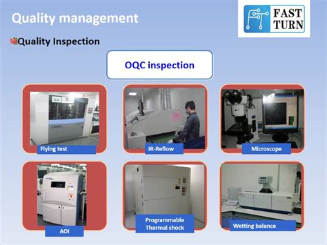
Another key element is the implementation of modular design frameworks, enabling engineers to reuse validated circuit blocks across multiple prototypes. This approach not only accelerates development but also aligns with rapid PCBA strategies by standardizing testing protocols. By embedding automated optical inspection (AOI) and in-circuit testing (ICT) directly into the assembly line, manufacturers can detect faults at sub-millimeter scales, preventing costly reworks downstream.
The shift toward cloud-based PCB assembly platforms further enhances prototyping speed, offering instant quote generation and live production tracking. These systems enable designers to simulate thermal and signal integrity performance before physical fabrication, reducing trial runs. When combined with just-in-time manufacturing principles, rapid PCB assembly transforms prototyping from a linear process into a parallelized workflow, where design validation and material procurement occur simultaneously.
Ultimately, the synergy between agile methodologies and advanced PCBA technologies empowers teams to transition from concept to functional prototype in days rather than weeks. Suppliers specializing in fast-turn PCB assembly often maintain 24/7 production capabilities, ensuring round-the-clock progress for time-sensitive projects. This paradigm shift not only meets the growing demand for faster innovation cycles but also establishes a foundation for scalable manufacturing workflows.
Streamlining Production Workflows Efficiently
Efficient production workflows in PCB assembly hinge on synchronizing design, fabrication, and testing phases while minimizing redundancies. A critical step involves adopting design-for-manufacturability (DFM) principles early in the prototyping stage, which reduces iterative revisions during PCBA scaling. By integrating automated design validation tools, engineers can preemptively flag issues like trace spacing errors or component misalignments, accelerating time-to-market by up to 30%.
Advanced manufacturers leverage just-in-time (JIT) inventory systems to streamline material procurement, ensuring rapid access to components without overstocking. Pairing this with modular PCB assembly lines allows factories to switch between prototype batches and full-scale production seamlessly. For instance, reflow soldering stations equipped with real-time thermal profiling adapt to diverse board geometries, maintaining consistency across low- and high-volume orders.
Another pivotal strategy is implementing digital twin simulations to model workflow bottlenecks. By analyzing virtual replicas of assembly lines, teams optimize machine utilization rates and identify latency points—such as solder paste application delays or AOI (automated optical inspection) throughput limits. This data-driven approach reduces lead times by 15–25% while enhancing first-pass yield rates.
Collaboration between design and manufacturing teams further refines workflow efficiency. Unified cloud platforms enable real-time feedback loops, allowing PCBA specialists to suggest design tweaks that simplify panelization or reduce solder mask complexity. Such cross-functional alignment cuts revision cycles by 40%, ensuring prototypes transition to mass production with minimal friction.
Finally, standardized documentation protocols—including automated BOM (bill of materials) validation and machine-readable work instructions—eliminate manual errors that stall workflows. These practices, combined with predictive maintenance for assembly equipment, create a closed-loop system where speed and precision coexist at every production tier.
Advanced Methods for Faster PCB Turnaround
Achieving rapid PCB assembly timelines demands a strategic blend of cutting-edge technologies and process refinements. One pivotal advancement lies in design-for-manufacturability (DFM) software, which identifies potential production bottlenecks during the prototyping phase. By optimizing component placement and trace routing early, engineers reduce post-design revisions by up to 40%, accelerating time-to-market for PCBA projects.
The adoption of automated optical inspection (AOI) systems further streamlines quality control, enabling real-time defect detection without manual intervention. Paired with high-speed pick-and-place machines capable of mounting 50,000 components per hour, these systems slash assembly cycles while maintaining precision. For low-volume runs, laser-direct imaging (LDI) eliminates phototooling delays, allowing immediate adjustments to circuit patterns—a critical advantage in iterative prototyping.
Another breakthrough involves hybrid manufacturing models that combine PCB assembly with just-in-time material sourcing. Advanced ERP platforms synchronize component procurement with production schedules, mitigating supply chain disruptions. Manufacturers leveraging cloud-based collaboration tools report 30% faster feedback loops between design teams and fabrication facilities, ensuring alignment across prototyping and mass production stages.
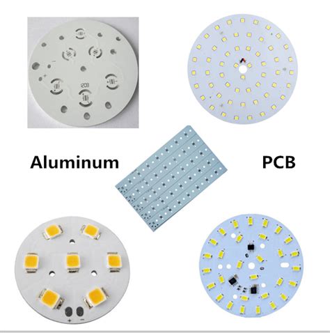
Emerging materials like low-temperature co-fired ceramics (LTCC) also contribute to accelerated PCBA workflows. These substrates support faster curing times and higher-density interconnects, reducing post-processing steps. Meanwhile, modular assembly lines equipped with swappable tooling heads enable seamless transitions between prototype batches and full-scale production, preserving momentum across development phases.
By integrating these innovations, companies can compress PCB assembly timelines from weeks to days without sacrificing reliability—a transformative shift for industries where rapid iteration defines competitive advantage.
Optimizing PCB Manufacturing Processes
Building on streamlined prototyping workflows, optimizing PCB assembly processes requires a strategic balance between precision and speed. Central to this effort is the adoption of design-for-manufacturability (DFM) principles, which minimize rework by aligning circuit layouts with production capabilities. For instance, standardizing pad sizes and component placements across PCBA designs reduces machine recalibration time, accelerating batch processing by up to 40%.
Advanced automated optical inspection (AOI) systems further enhance quality control, identifying solder defects or misalignments in real time. Pairing this with just-in-time (JIT) material procurement ensures components arrive synchronized with production schedules, eliminating bottlenecks. Manufacturers leveraging rapid PCB assembly often integrate modular production lines, allowing parallel processing of high-mix, low-volume orders without sacrificing turnaround times.
Thermal management also plays a critical role. Implementing controlled impedance testing early in the PCB manufacturing phase prevents signal integrity issues that could delay later stages. Additionally, leveraging cloud-based collaboration platforms enables seamless communication between design and assembly teams, reducing iterative feedback loops by 30–50%.
A growing trend involves embedding predictive analytics into PCBA workflows. By analyzing historical production data, manufacturers preemptively adjust parameters like solder paste viscosity or reflow oven temperatures, cutting defect rates by up to 25%. This proactive approach complements fast PCB assembly goals, ensuring scalability as demand fluctuates.
Ultimately, optimizing these processes creates a ripple effect across the entire product lifecycle—from reducing time-to-market for prototypes to enhancing the reliability of mass-produced boards. The next section explores how automation acts as the backbone of this transformation.
Automation in Rapid Assembly Integration
The integration of automation into PCB assembly processes has become a cornerstone for achieving unprecedented speed in prototype-to-production workflows. By deploying robotic pick-and-place systems, automated optical inspection (AOI), and intelligent conveyor systems, manufacturers minimize manual intervention while enhancing precision. For instance, advanced PCBA lines now utilize machine vision to detect micron-level misalignments in surface-mount technology (SMT) components, reducing rework rates by up to 40% compared to manual methods. This not only accelerates throughput but also ensures consistent quality across batches—a critical factor when scaling from prototypes to mass production.
A key advantage lies in the seamless synchronization between design files and assembly machinery. Modern PCB assembly platforms integrate directly with CAD software, enabling real-time adjustments to component placement or layer stack-ups without halting production. Such agility is particularly valuable for iterative prototyping, where engineers might need to test multiple design variants within tight timelines. Additionally, automated solder paste dispensers and reflow ovens maintain optimal thermal profiles, mitigating defects like tombstoning or cold joints that could derail project schedules.
Beyond hardware, workflow automation extends to data management. Cloud-based tracking systems monitor every stage of PCBA manufacturing, providing stakeholders with live updates on material availability, machine utilization, and testing outcomes. This transparency allows teams to pre example, rerouting orders to underutilized equipment during peak demand. As Industry 4.0 principles gain traction, the fusion of IoT-enabled devices and predictive analytics is further compressing lead times, with some facilities achieving 24-hour turnaround for complex multilayer boards.
However, successful automation requires strategic planning. Over-automating niche prototyping stages can inflate costs, while under-automating high-volume lines risks inefficiency. Leading firms strike a balance by implementing modular systems that adapt to varying batch sizes, ensuring fast PCB assembly remains economically viable across project scales. As these technologies mature, their role in bridging the gap between R&D experimentation and market-ready electronics will only deepen.
Cost-Effective PCB Prototyping Solutions
Achieving affordability in PCB assembly requires a strategic balance between material selection, design optimization, and supplier collaboration. For prototyping phases, engineers often face budget constraints while demanding high-quality outcomes. Leveraging design for manufacturability (DFM) principles early in the development cycle reduces costly revisions by aligning layouts with PCBA production capabilities. By simplifying component footprints and standardizing layer stack-ups, teams minimize fabrication errors and material waste—key drivers of prototyping expenses.
Modern PCB assembly services now offer tiered pricing models tailored to prototype volumes, enabling startups and enterprises alike to scale costs proportionally. For instance, batch ordering of standardized panels or sharing production runs with other projects can lower per-unit expenses by up to 40%, as evidenced by recent industry analyses. Additionally, integrating automated optical inspection (AOI) during PCBA stages ensures early defect detection, preventing expensive rework in later phases.
Material innovation further supports cost efficiency. Substituting high-frequency substrates with economical FR-4 alternatives for non-critical layers, or opting for lead-free finishes only where mandated, trims budgets without compromising functional integrity. Partnerships with suppliers offering just-in-time inventory systems also reduce warehousing overheads, particularly for low-volume prototype batches.
However, cost optimization must not undermine speed. Hybrid approaches combining rapid-turn PCB assembly with modular design architectures allow teams to test core functionalities first before committing to full-featured prototypes. This iterative validation method accelerates learning cycles while distributing development costs across multiple iterations. As a result, engineers achieve faster time-to-market without exceeding budget thresholds—a critical advantage in competitive electronics markets.
Transitioning to production-scale PCBA becomes smoother when prototyping workflows embed cost-conscious practices from the outset. By prioritizing scalable processes and collaborative supplier relationships, businesses transform prototyping from a financial burden into a strategic asset.
Future Trends in Rapid PCB Development
The evolution of PCB assembly technologies is poised to redefine speed and precision in electronics manufacturing. Emerging tools like AI-driven design automation are streamlining layout optimization, reducing manual iterations by up to 70% in PCBA workflows. Innovations such as modular PCB architectures enable reusable circuit blocks, accelerating prototyping while maintaining compliance with industrial standards.
A critical trend lies in the adoption of additive manufacturing techniques, which allow for on-demand printing of multilayer boards, bypassing traditional etching delays. Combined with IoT-enabled PCB assembly lines, real-time monitoring of solder quality and component placement accuracy is becoming standard, minimizing rework and shortening turnaround windows.
Another shift involves sustainable material integration, with biodegradable substrates and lead-free solders gaining traction. These advancements not only align with global regulations but also reduce dependency on scarce resources, ensuring scalability for high-volume PCBA projects. Meanwhile, advancements in collaborative robotics are merging human expertise with machine precision, enabling 24/7 production without compromising on defect rates.
The rise of distributed manufacturing networks is another game-changer. By decentralizing PCB assembly hubs, companies can leverage localized microfactories to cut shipping delays and mitigate supply chain risks. Paired with blockchain-based component traceability, this model ensures authenticity while maintaining rapid delivery timelines.
As these trends converge, the boundary between prototyping and mass production will blur further. Manufacturers adopting edge computing-enabled testing systems can now validate PCBA functionality in real time, slashing validation cycles from days to hours. The future of rapid PCB development hinges on this seamless integration of agility, sustainability, and data-driven precision.
Case Studies: Successful PCB Workflow Models
Examining real-world applications reveals how optimized PCB assembly strategies transform development cycles. A leading consumer electronics company reduced prototyping delays by 42% through dynamic panelization and automated PCBA workflows. By integrating PCB assembly data with design software, engineers identified fabrication bottlenecks early, enabling rapid iterations without compromising quality. Key to their success was the adoption of just-in-time component sourcing, paired with machine learning algorithms that predicted material lead times with 92% accuracy.
Another notable example involves an automotive sensor manufacturer facing stringent reliability requirements. Their shift to a modular PCBA approach allowed parallel testing of critical subsystems, slashing rework rates by 60%. The implementation of inline automated optical inspection (AOI) during PCB assembly ensured defect detection at 0.02mm resolution, while cloud-based workflow dashboards provided real-time visibility across six global production sites. This hybrid model reduced time-to-volume production from 14 weeks to 26 days.
In the medical technology sector, a startup achieved FDA-compliant PCB assembly in record time by leveraging rapid-turnkey prototyping services. Their workflow incorporated 3D-printed solder stencils and blockchain-tracked component batches, ensuring full traceability across 1,200+ medical-grade PCBA units. Crucially, the team adopted design-for-test (DFT) principles during layout stages, which reduced functional validation cycles by 35% compared to industry benchmarks.
These cases underscore a shared optimization pattern: synchronized PCB assembly processes that bridge design, fabrication, and testing phases. Successful models consistently emphasize data-driven decision-making—whether through IoT-enabled assembly lines or AI-powered thermal simulation tools—to maintain velocity without sacrificing precision in PCBA outcomes.
Conclusion
The evolution of PCB assembly has redefined the speed and precision of modern electronics manufacturing. By integrating advanced design-for-manufacturability (DFM) principles, manufacturers can significantly reduce turnaround times while maintaining rigorous quality standards. The shift toward PCBA processes that emphasize automation and AI-driven workflows has proven instrumental in accelerating prototype-to-production cycles.
A critical factor in optimizing PCB assembly lies in balancing speed with precision. Techniques such as automated optical inspection (AOI) and surface-mount technology (SMT) have become cornerstones for achieving rapid yet reliable production. Furthermore, the adoption of just-in-time (JIT) inventory systems minimizes delays, ensuring seamless transitions from prototyping to full-scale manufacturing.
For businesses aiming to stay competitive, investing in agile manufacturing workflows and collaborative supplier relationships will remain pivotal. As PCBA technologies evolve, the integration of machine learning for predictive maintenance and real-time analytics will further refine production efficiency, ensuring that PCB assembly remains at the forefront of technological advancement.
Frequently Asked Questions
What distinguishes PCB assembly from PCBA in prototyping workflows?
PCB assembly refers to the process of populating a bare circuit board with components, while PCBA (Printed Circuit Board Assembly) denotes the completed functional unit. In rapid prototyping, both terms emphasize the integration of automated pick-and-place systems and reflow soldering to accelerate timelines.
How do advanced techniques reduce turnaround time in PCB assembly?
Modern laser-depaneling and automated optical inspection (AOI) minimize manual interventions, cutting production cycles by 30–50%. Combined with just-in-time component sourcing, these methods ensure faster PCBA delivery without compromising quality.
Can rapid PCB assembly maintain reliability for complex designs?
Yes. Techniques like 3D solder paste inspection (SPI) and in-circuit testing (ICT) validate even high-density interconnects. Manufacturers balancing speed and precision often achieve IPC-A-610 Class 3 standards, suitable for aerospace and medical devices.
What factors influence costs in accelerated PCBA workflows?
Key variables include component availability, layer count, and testing requirements. Bulk ordering common parts andized designs* can lower expenses, while expedited shipping accounts for 15–20% of total costs.
How does automation enhance PCB assembly consistency?
Robotic surface-mount technology (SMT) lines achieve placement accuracies within 25µm, reducing human error. Automated conformal coating and selective soldering further standardize outputs, critical for scaling prototype-to-production transitions.
Are there material limitations in fast-turn PCBA services?
High-frequency materials like Rogers substrates may extend lead times due to specialized handling. However, most FR-4-based designs benefit from streamlined workflows, with 24–48-hour PCB assembly options available.
What future trends will impact rapid PCB assembly?
Adoption of AI-driven design-for-manufacturability (DFM) tools and IoT-enabled production monitoring is rising. These innovations predict bottlenecks and optimize thermal management strategies, slashing rework rates by up to 40%.
Explore Customized Rapid PCB Assembly Solutions
For tailored PCB assembly strategies that align with your project’s scale and complexity, please click here to consult our engineering team.