Rapid PCB Prototyping: Revolutionizing Electronics Design and Manufacturing
Introduction
In the fast-paced world of electronics, the ability to quickly design, test, and iterate on printed circuit boards (PCBs) is crucial for staying competitive. Rapid PCB prototyping has emerged as a game-changing approach, enabling engineers and designers to accelerate the development process, reduce costs, and bring innovative products to market faster than ever before. This article explores the concept of rapid PCB prototyping, its benefits, the technologies driving it, and its impact on the electronics industry.
What is Rapid PCB Prototyping?
Rapid PCB prototyping refers to the process of quickly creating functional prototypes of printed circuit boards for testing and validation purposes. Unlike traditional PCB manufacturing, which can take weeks or even months, rapid prototyping allows for the production of PCBs in a matter of days or even hours. This speed is achieved through the use of advanced manufacturing technologies, streamlined design processes, and the integration of software tools that facilitate rapid iteration.
The goal of rapid PCB prototyping is to enable engineers to test their designs, identify potential issues, and make necessary adjustments before moving to full-scale production. This iterative approach reduces the risk of costly errors and ensures that the final product meets the desired specifications.
The Benefits of Rapid PCB Prototyping
- Faster Time-to-Market: One of the most significant advantages of rapid PCB prototyping is the ability to bring products to market more quickly. By reducing the time required for design iterations and testing, companies can accelerate their development cycles and gain a competitive edge.
- Cost Savings: Rapid prototyping helps reduce costs by minimizing the need for expensive tooling and long lead times associated with traditional PCB manufacturing. Additionally, identifying and resolving design issues early in the process prevents costly rework during full-scale production.
- Improved Design Quality: The iterative nature of rapid prototyping allows engineers to test multiple design variations and optimize their PCBs for performance, reliability, and manufacturability. This leads to higher-quality end products that are less likely to fail in the field.
- Enhanced Collaboration: Rapid prototyping facilitates better collaboration between design, engineering, and manufacturing teams. By providing physical prototypes early in the design process, teams can communicate more effectively and make informed decisions based on real-world testing.
- Flexibility and Customization: Rapid prototyping enables greater flexibility in design, allowing engineers to experiment with different layouts, components, and materials. This is particularly valuable for custom or low-volume production runs where traditional manufacturing methods may not be cost-effective.
Technologies Driving Rapid PCB Prototyping
Several key technologies have played a pivotal role in enabling rapid PCB prototyping:
- Computer-Aided Design (CAD) Software: Modern CAD tools have revolutionized the way PCBs are designed. These software platforms allow engineers to create detailed schematics and layouts, simulate circuit behavior, and generate manufacturing files with unprecedented speed and accuracy. Popular CAD tools include Altium Designer, KiCad, and Eagle.
- 3D Printing and Additive Manufacturing: While traditional PCB manufacturing relies on subtractive processes (e.g., etching copper layers), 3D printing and additive manufacturing techniques are increasingly being used for rapid prototyping. These methods enable the creation of complex, multi-layer PCBs with embedded components, reducing the need for manual assembly.
- Direct Imaging and Laser Etching: Direct imaging systems use lasers to precisely pattern conductive traces on PCB substrates, eliminating the need for photomasks and reducing production time. Laser etching is also used for rapid prototyping of flexible and rigid-flex PCBs, which are becoming more common in modern electronics.
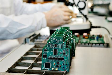
- Automated Assembly and Pick-and-Place Machines: Automated assembly systems, including pick-and-place machines, have streamlined the process of populating PCBs with components. These machines can quickly and accurately place surface-mount devices (SMDs) on prototype boards, reducing the time and labor required for manual assembly.
- Rapid Turnaround PCB Fabrication Services: A growing number of specialized PCB fabrication services offer rapid turnaround times, often delivering prototypes within 24 to 48 hours. These services leverage advanced manufacturing techniques and economies of scale to provide high-quality PCBs at competitive prices.
The Rapid PCB Prototyping Process
The rapid PCB prototyping process typically involves the following steps:
- Design and Schematic Capture: Engineers begin by creating a schematic of the circuit using CAD software. This schematic defines the electrical connections between components and serves as the blueprint for the PCB layout.
- PCB Layout and Routing: Using the schematic as a guide, engineers design the physical layout of the PCB, including the placement of components and the routing of conductive traces. Modern CAD tools often include auto-routing features that optimize the layout for performance and manufacturability.
- Design Verification and Simulation: Before proceeding to fabrication, the design is verified using simulation tools to ensure that it meets electrical and thermal requirements. This step helps identify potential issues early in the process.
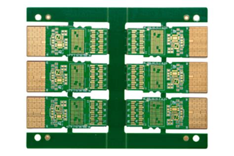
- Prototype Fabrication: Once the design is finalized, the PCB is fabricated using rapid prototyping techniques. This may involve direct imaging, laser etching, or additive manufacturing, depending on the complexity of the design.
- Assembly and Testing: After fabrication, the prototype PCB is populated with components using automated assembly systems or manual techniques. The assembled board is then tested to verify its functionality and performance.
- Iteration and Optimization: Based on the test results, engineers may make adjustments to the design and repeat the prototyping process until the PCB meets all requirements.
Applications of Rapid PCB Prototyping
Rapid PCB prototyping has found applications across a wide range of industries, including:
- Consumer Electronics: Companies developing smartphones, wearables, and other consumer devices rely on rapid prototyping to quickly iterate on designs and stay ahead of market trends.
- Automotive: The automotive industry uses rapid prototyping to develop advanced driver-assistance systems (ADAS), infotainment systems, and electric vehicle (EV) components.
- Medical Devices: Rapid prototyping is essential for the development of medical devices, where precision and reliability are critical. Examples include implantable devices, diagnostic equipment, and wearable health monitors.
- Aerospace and Defense: In the aerospace and defense sectors, rapid prototyping enables the development of high-performance avionics, communication systems, and unmanned aerial vehicles (UAVs).
- Internet of Things (IoT): The IoT industry benefits from rapid prototyping by enabling the rapid development of connected devices, sensors, and edge computing solutions.
Challenges and Future Trends
While rapid PCB prototyping offers numerous advantages, it also presents certain challenges:
- Material Limitations: Some advanced materials used in high-performance PCBs may not be compatible with rapid prototyping techniques, limiting their applicability in certain industries.
- Cost of Equipment: The initial investment in rapid prototyping equipment, such as 3D printers and laser etching systems, can be prohibitive for small companies or startups.
- Skill Requirements: Rapid prototyping requires specialized knowledge and skills, particularly in CAD software and additive manufacturing techniques. Companies may need to invest in training to fully leverage these technologies.
Looking ahead, several trends are expected to shape the future of rapid PCB prototyping:
- Increased Adoption of Additive Manufacturing: As additive manufacturing technologies continue to advance, they are likely to play an even greater role in rapid PCB prototyping, enabling the creation of more complex and integrated designs.
- AI-Driven Design Tools: Artificial intelligence (AI) is poised to revolutionize PCB design by automating tasks such as component placement, routing, and optimization. This will further accelerate the prototyping process and improve design quality.
- Sustainability: The electronics industry is increasingly focused on sustainability, and rapid prototyping can contribute by reducing material waste and energy consumption. Future developments may include the use of eco-friendly materials and processes.
- Integration with Industry 4.0: Rapid PCB prototyping is expected to become more integrated with Industry 4.0 technologies, such as the Internet of Things (IoT) and big data analytics. This will enable real-time monitoring and optimization of the prototyping process.
Conclusion
Rapid PCB prototyping has transformed the way electronics are designed and manufactured, offering significant benefits in terms of speed, cost, and quality. By leveraging advanced technologies such as CAD software, additive manufacturing, and automated assembly, companies can bring innovative products to market faster and more efficiently than ever before. As the electronics industry continues to evolve, rapid prototyping will play an increasingly important role in driving innovation and maintaining a competitive edge
.


