Rapid Prototyping Solutions for Single PCB Production

Key Takeaways
When exploring PCB manufacturing for single-unit projects, understanding your options can save time and resources. First, in-house prototyping empowers you to bypass lead times from PCB manufacturing companies, particularly when iterating custom designs like keyboard circuits. While traditional fabrication excels at bulk orders, creating one-off boards often requires overcoming etching precision issues—common hurdles in DIY processes.
Second, PCB manufacturing cost for single units becomes manageable with optimized material usage and alternative etching techniques. Chemical concentration control and laser-printed transfers reduce errors that typically inflate expenses. For those running a small PCB manufacturing business, mastering these methods improves margins while maintaining quality.
Third, speed-focused strategies—such as UV exposure setups or pre-sensitized boards—compress production timelines from weeks to hours. This approach proves vital when testing functional prototypes under real-world conditions. However, balancing speed with accuracy remains critical; rushed etching can create trace discontinuities that demand costly reworks.
Finally, comparing in-house vs. outsourced fabrication reveals trade-offs. While external partners offer advanced finishes like ENIG plating, their minimum order quantities often clash with single-PCB needs. Hybrid workflows—where you prototype internally before engaging manufacturers—strike a practical balance. Always document troubleshooting steps for common issues (e.g., overdeveloped resist layers) to refine your process iteratively.
By aligning techniques with project-specific demands, you’ll navigate the complexities of PCB manufacturing without compromising on turnaround or functionality.
In-House PCB Prototyping for Single Units
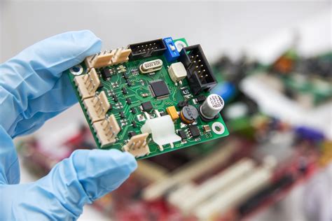
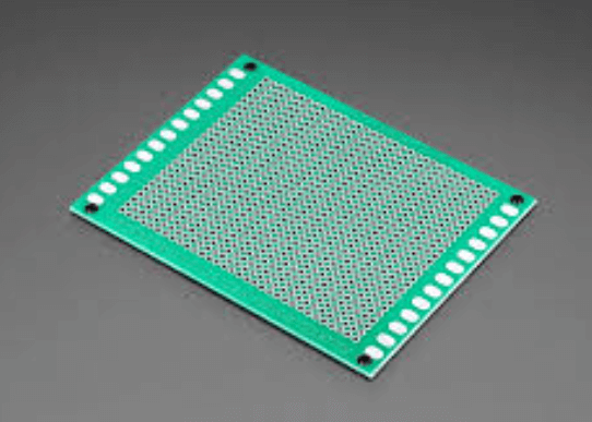
When creating single-unit PCB prototypes, in-house methods let you bypass the lead times and pcb manufacturing cost structures of traditional fabrication. By leveraging accessible tools like laser printers and UV exposure units, you can produce functional boards within hours instead of weeks. This approach is particularly valuable for custom projects like keyboard PCBs, where iterative design changes demand rapid testing cycles.
A typical in-house workflow involves:
- Printing circuit patterns onto transparent film
- Transferring designs to copper-clad boards via UV exposure
- Chemical etching using ferric chloride or alternative solutions
- Precision drilling for component placement
| Method | Tools Required | Time Investment | Material Cost |
|---|---|---|---|
| UV Exposure | Transparent film, UV chamber | 2-3 hours | $15-$30 |
| Toner Transfer | Laser printer, laminator | 1.5 hours | $10-$20 |
| CNC Milling | Desktop mill, CAD software | 4-6 hours | $50-$100 |
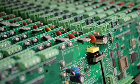
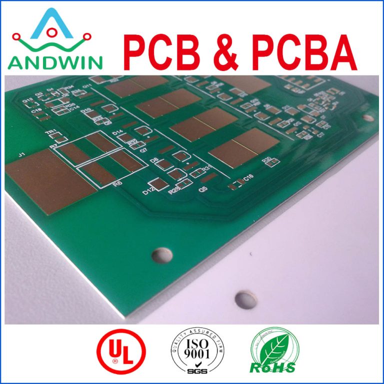
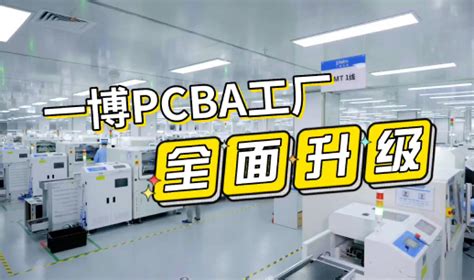
While pcb manufacturing companies excel at bulk production, their minimum order quantities often make single-unit requests impractical. For instance, outsourcing a single keyboard PCB might cost $200+ through traditional channels, whereas in-house prototyping reduces this to under $50. The pcb manufacturing business model prioritizes scale, but modern tools like solder paste stencils and reflow ovens now enable lab-grade results in home workshops.
Key advantages of DIY prototyping include:
- Immediate design validation for complex layouts
- Cost avoidance of NRE (non-recurring engineering) fees
- Flexibility to test alternative trace geometries
However, troubleshooting etching inconsistencies or alignment errors requires patience. For mission-critical projects, hybrid approaches work best: prototype in-house, then partner with professional services like Andwin PCBA for final production. This balances speed with the reliability of established pcb manufacturing processes.
Overcoming Etching Challenges in DIY PCBs
When creating single-unit PCBs in-house, etching remains one of the most technically demanding stages. Unlike PCB manufacturing companies that use industrial-grade chemical baths and precision masking, DIY setups require meticulous control to avoid over-etching (which thins traces) or under-etching (leaving conductive artifacts). To address this, start by calibrating your etching solution—typically ferric chloride or ammonium persulfate—to maintain optimal temperature (20–25°C). Cold solutions slow the reaction, increasing the risk of uneven copper removal, while excessive heat accelerates etching beyond manageable limits.
For consistent results, use a laminator to ensure photoresist film adheres uniformly to the copper-clad board. Even minor air bubbles can create weak spots in the mask, leading to broken traces. If you’re working with toner transfer paper, pre-treat the board with fine-grit sandpaper to improve adhesion. Post-etching, inspect traces under bright light and magnify them to identify micro-shorts or hairline fractures—common culprits of prototyping errors.
Time management is critical. Unlike traditional PCB manufacturing, where automated systems handle timing, DIY etching demands manual oversight. Set a timer for 5–7 minutes, agitating the tank gently to prevent stagnation. After rinsing, immediately neutralize the solution with baking soda to halt the reaction. This step not only preserves the board but also reduces chemical waste, aligning with cost-efficient PCB manufacturing business practices.
While DIY etching saves on PCB manufacturing cost for single boards, recognize its limitations. Complex designs with <0.2mm trace widths or tight spacing may still require professional fabrication. However, mastering these techniques allows you to iterate rapidly for projects like custom keyboard PCBs, bypassing lead times from external suppliers. Remember: each successful etch brings you closer to refining a process that balances speed, precision, and repeatability—cornerstones of effective in-house prototyping.
Fast-Track Methods for Single PCB Creation
When implementing PCB manufacturing for single-unit projects, speed hinges on optimizing design-to-production workflows. Start by leveraging direct printing systems like inkjet or laser methods, which bypass traditional photoresist steps. These systems enable rapid trace patterning—often in under an hour—by depositing conductive ink or ablating copper directly onto substrates. For complex layouts, consider CNC milling to carve traces from pre-clad boards, though ensure spindle speeds exceed 24,000 RPM to minimize burring.
Tip: Pair milling machines with vacuum beds to stabilize thin substrates during high-speed machining, reducing alignment errors by up to 70%.
If chemical etching remains unavoidable, use ferric chloride alternatives like ammonium persulfate for faster reaction times. Preheated solutions (40–50°C) can slash etching durations to 3–5 minutes while maintaining trace integrity. Always prioritize ventilation and neutralize waste fluids to comply with environmental regulations—a critical factor when scaling a PCB manufacturing business.
For designers requiring immediate validation, hybrid approaches combine milled prototypes with hand-soldered components. This method avoids the 2–3-week lead times typical of PCB manufacturing companies, though it demands precision in drilling micro-vias (≤0.3mm). To offset PCB manufacturing cost, repurpose failed prototypes: salvage undamaged ICs or reuse substrates for less critical layers.
Suggestion: Create modular jigs for recurring designs—pre-aligned fixtures cut setup time by 30% per iteration, especially for custom keyboard PCBs with standardized footprints.
Digital verification tools further accelerate iterations. Run real-time DFM checks to flag clearance violations or impedance mismatches before physical production. Open-source ECAD plugins like KiBot automate Gerber generation, reducing file export errors that cause 22% of prototyping delays. When outsourcing becomes necessary, opt for local rapid-turn services offering 24-hour fabrication—ideal for verifying high-frequency signal paths without overhauling your in-house workflow.
By balancing speed-oriented techniques with cost controls, single-board prototyping evolves from a bottleneck into a strategic advantage, particularly for niche applications where traditional PCB manufacturing timelines clash with urgent design cycles.
Cost-Effective Single Board Fabrication Techniques
When optimizing PCB manufacturing cost for single-board projects, material selection becomes your first strategic decision. Low-cost substrates like FR-4 remain popular for prototyping, but advanced composites can reduce waste in specialized applications. By refining your design to minimize board dimensions and layer counts, you’ll inherently lower material usage—a critical factor when PCB manufacturing companies calculate pricing based on panel utilization.
For DIY enthusiasts, toner transfer methods offer surprising precision at a fraction of traditional fabrication expenses. Pair this with affordable UV-curable soldermasks to achieve professional-grade finishes without outsourcing. If chemical etching feels daunting, consider partnering with local PCB manufacturing businesses that offer small-batch services—many now provide tiered pricing models tailored for single-unit production.
Software optimization further slashes costs. Leveraging open-source EDA tools eliminates licensing fees, while design rule checks (DRCs) prevent costly errors before fabrication. When evaluating PCB manufacturing cost, remember that simplified layouts with fewer vias and standardized drill sizes reduce machining time. For projects requiring precise tolerances, hybrid approaches—combining in-house etching with outsourced drilling—strike a balance between quality and affordability.
Finally, bulk-purchasing commonly used components like copper-clad boards or etchants creates long-term savings, even for one-off builds. Always compare lead times and MOQs (Minimum Order Quantities) across multiple PCB manufacturing companies to identify hidden value—some providers waive setup fees for single-layer designs under specific size thresholds. By integrating these strategies, you transform prototyping from a costly necessity into a streamlined, budget-conscious process.
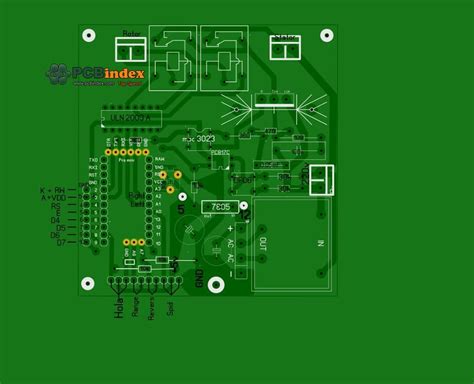
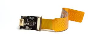
DIY Keyboard PCB Design Best Practices
When designing a PCB manufacturing-ready layout for custom keyboards, precision begins with component placement. Start by positioning switches and controllers to minimize trace lengths, ensuring signal integrity while avoiding interference hotspots. Use routing tools in your design software to create clean paths for high-speed signals, such as USB-C connections, and prioritize ground planes to reduce electromagnetic noise—a common pitfall in compact DIY layouts.
Material selection directly impacts PCB manufacturing cost and durability. For single-board prototypes, opt for 1.6mm FR4 substrates unless your design requires specialized materials like polyimide for flexibility. Double-check pad sizes for switch sockets; undersized pads risk detachment during soldering, while oversized ones may bridge connections. Impedance matching becomes critical if integrating RGB lighting or wireless modules, as mismatched traces can degrade performance.
To avoid delays often associated with traditional PCB manufacturing companies, leverage design-for-manufacturing (DFM) checks in tools like KiCad or Eagle. These tools flag errors like insufficient clearance between traces or missing solder masks—issues that could force costly revisions. For complex designs, consider partnering with a PCB manufacturing business specializing in low-volume orders, as they often provide pre-production feedback to refine your files.
Thermal management is frequently overlooked in DIY projects. Ensure power-hungry components like microcontrollers have adequate copper pours or thermal vias to dissipate heat. If hand-soldering, use reflow-friendly footprints (e.g., drag-and-drop compatible pads) to simplify assembly. Finally, validate your design with a breadboard prototype before committing to fabrication—this step catches logical errors that software simulations might miss, saving both time and material costs.
Balancing creativity with practicality ensures your single-board keyboard PCB transitions smoothly from concept to functional prototype, whether you’re iterating in-house or collaborating with external partners.

In-House vs Traditional PCB Fabrication Timelines
When evaluating timelines for single-board projects, understanding the trade-offs between PCB manufacturing in-house and outsourcing to PCB manufacturing companies becomes critical. While traditional fabrication services often require 5-15 business days for delivery—excluding shipping and design review phases—a DIY approach lets you bypass queue delays entirely. This difference becomes stark when prototyping custom keyboard layouts, where iterative adjustments might demand multiple revisions.
Traditional workflows involve design submission, material sourcing, and third-party quality checks, all contributing to extended lead times. PCB manufacturing cost structures in these scenarios typically prioritize bulk orders, making single-unit requests economically inefficient. By contrast, in-house methods using direct laser imaging or UV exposure systems enable same-day turnaround, though they require upfront investments in equipment like etching tanks and laminators.
However, speed isn’t the sole factor. Consistency in trace quality and via plating remains a challenge for DIY setups, especially when replicating multilayer designs common in PCB manufacturing business standards. For instance, thermal management in compact keyboard PCBs often demands precision that hobbyist-grade tools might struggle to achieve reliably.
Transitioning between these approaches depends on your project’s phase. Initial prototyping benefits from rapid in-house iterations, while final production batches may justify traditional vendors’ longer timelines for guaranteed industrial-grade outputs. Balancing time-sensitive experimentation with scalability requirements ensures you avoid bottlenecks—whether from overburdened PCB manufacturing companies during peak seasons or unexpected etching errors in DIY workflows.
Ultimately, the choice hinges on aligning your timeline expectations with technical capabilities. For single-board needs where hours matter more than perfection, in-house fabrication offers autonomy. For complex designs requiring certification or high-frequency performance, traditional services provide peace of mind—even with added waiting periods.
Troubleshooting Common Prototyping Errors
When creating PCB manufacturing prototypes in-house, even minor oversights can lead to frustrating setbacks. Inconsistent etching often tops the list of issues, particularly when using chemical methods for single-board projects. If traces appear partially dissolved or uneven, check your exposure time and UV light alignment—overexposure weakens resist layers, while underexposure leaves copper unetched. For PCB manufacturing cost efficiency, calibrate chemical concentrations precisely; overly diluted ferric chloride slows etching, risking overcutting on delicate traces.
Another frequent error involves soldering bridges between tightly spaced components. This becomes critical in custom keyboard designs where switch footprints cluster near microcontroller pads. Use flux-core solder and a fine-tip iron to maintain precision, and inspect connections under magnification before testing continuity. If you encounter unexplained shorts, double-check your design files for accidental overlaps in ground planes or power rails—a common oversight when repurposing templates for rapid prototyping.
Thermal management issues often surface during functional testing, especially when using low-cost substrates. Warping or delamination under heat stress signals inadequate material selection. While PCB manufacturing companies typically use FR4 for its thermal resilience, DIY prototypes might employ cheaper alternatives. If board flexibility is essential (e.g., for split keyboard designs), prioritize polyimide substrates but account for their lower heat tolerance during soldering.
For trace width miscalculations, leverage free design rule check (DRC) tools to validate current-carrying capacities before printing. A 0.3mm trace might suffice for signal paths but could overheat in power delivery sections. When iterating designs, document each revision’s voltage/current requirements to build a troubleshooting reference library—this reduces debugging time for future PCB manufacturing business projects.
Finally, if prototyping delays persist despite meticulous efforts, reassess your workflow against traditional fabrication timelines. While in-house methods excel for single-unit urgency, complex multilayer designs might justify outsourcing to balance PCB manufacturing cost and reliability. Use prototyping errors as diagnostic tools: recurring soldering flaws could indicate the need for better stencils, while consistent etching failures might warrant investment in a precision exposure unit.
Conclusion
When navigating the complexities of PCB manufacturing for single-unit projects, balancing speed, precision, and PCB manufacturing cost becomes critical. While traditional PCB manufacturing companies excel at bulk orders, their timelines and minimum quantity requirements often clash with rapid prototyping needs—especially for niche applications like custom keyboard designs. By adopting in-house methods, you bypass delays associated with external vendors, gaining full control over iterative adjustments and material choices.
However, this approach demands careful consideration of etching precision and material waste. Techniques such as UV exposure or laser-printed transfers mitigate common errors, but mastering these requires practice. For highly specialized designs, partnering with a PCB manufacturing business that offers low-volume services might still be cost-effective, particularly if your design involves multi-layer boards or advanced substrates.
The decision ultimately hinges on your project’s urgency, complexity, and budget. Low-risk prototypes with simple layouts thrive in DIY environments, while intricate designs may warrant professional fabrication despite longer lead times. By understanding the trade-offs between in-house agility and industrial-grade consistency, you can strategically align your workflow with both technical requirements and financial constraints.
FAQs
How does in-house prototyping compare to using professional PCB manufacturing companies?
While professional PCB manufacturing services excel at bulk production, creating a single board yourself avoids minimum order quantities and shipping delays. For urgent revisions or niche designs (like custom keyboards), DIY methods provide immediate iteration control.
What factors influence PCB manufacturing cost for one-off projects?
Material selection, board complexity, and tool accessibility dominate expenses. In-house production eliminates setup fees charged by PCB manufacturing business providers but requires upfront investment in etching chemicals and precision tools. Commercial services may become cost-effective for multilayer designs or advanced finishes.
Can homemade PCBs match the quality of industrial-grade boards?
For simple two-layer designs, careful etching achieves functional results. However, high-density interconnects or impedance-controlled traces typically require professional PCB manufacturing equipment. Thermal management and solder mask application remain challenging in DIY setups.
When should you transition from prototyping to full-scale production?
If your design requires rigorous certification (e.g., FCC compliance) or involves 6+ layers, partnering with established PCB manufacturing companies becomes essential. Batch orders above 50 units often justify traditional fabrication despite longer lead times.
How do you troubleshoot inconsistent etching results?
Uneven copper removal usually stems from temperature fluctuations in the ferric chloride solution. Maintain the etch bath at 40-50°C and agitate continuously. Test with sacrificial boards first, and always use laser-printed transparency films for accurate mask alignment.
Ready to Scale Your Prototype?
For designs requiring advanced capabilities beyond DIY methods, click here to explore professional PCB manufacturing solutions that balance speed, precision, and cost-efficiency for both prototypes and production runs.