Revolutionizing Electronics: The Future of PCB Manufacturing
Key Takeaways
“Revolutionizing Electronics: The Future of PCB Manufacturing” clearly illustrates the transformative innovations reshaping the world of PCB manufacturing. As PCB manufacturing companies adopt advanced technologies like high-density interconnect (HDI) and 3D printing, they achieve more efficient designs and enhanced product reliability. Automation and state-of-the-art software tools are not only streamlining the production process but also significantly reducing PCB manufacturing cost. The article also highlights the importance of sustainable practices that are being integrated into the PCB manufacturing business, making it more environmentally friendly. These advancements are critical as they underpin the next generation of electronic devices, ensuring that products not only meet but exceed consumer expectations.
Introduction to Modern PCB Manufacturing
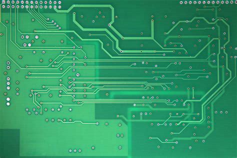
In today’s rapidly evolving electronics industry, PCB manufacturing plays a critical role in the creation of advanced technological devices. Modern methods and approaches have transformed the PCB manufacturing business, making it more efficient and innovative than ever before. With the integration of high-density interconnect (HDI) technology, manufacturers can now design more compact and complex circuits, significantly enhancing performance and functionality. Additionally, the adoption of cutting-edge techniques such as 3D printing is revolutionizing how PCBs are produced, offering new possibilities for customization and rapid prototyping.
One of the key aspects that have driven these advancements is automation. By utilizing state-of-the-art machinery and software tools, pcb manufacturing companies are able to streamline processes, reducing production time and minimizing human error. This not only increases efficiency but also helps in controlling the pcb manufacturing cost, making it more accessible for various applications.
Moreover, sustainable practices are becoming a focal point within the industry. Manufacturers are increasingly adopting environmentally friendly methods to reduce waste and improve energy efficiency, leading to a greener future for electronics production. This shift towards sustainability is not only beneficial for the environment but also enhances the overall reputation and marketability of PCB manufacturing companies.
Overall, modern PCB manufacturing is characterized by its innovative approaches, cost-effectiveness, and commitment to sustainability. As these trends continue to evolve, they will undoubtedly shape the future of electronic devices, ensuring that they meet both current demands and future challenges effectively.
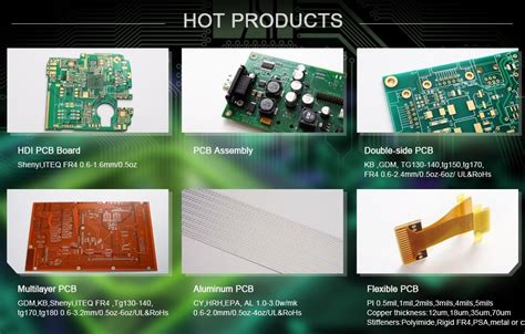
Advancements in High-Density Interconnect (HDI) Technology
HDI technology has become a cornerstone in modern pcb manufacturing, offering unparalleled advantages in circuit design and functionality. By enabling more complex routing on fewer layers, HDI boards significantly reduce the overall pcb manufacturing cost while maximizing space efficiency. One of the key features of HDI is the use of microvias, which allows for finer lines and spaces, leading to higher circuit density.
“Adopting HDI technology can be a game-changer for your pcb manufacturing business, as it fosters innovation and enhances product performance.”
In addition to cost savings, HDI also contributes to better signal integrity and improved thermal management. These benefits make HDI an attractive option for pcb manufacturing companies aiming to stay ahead in the competitive electronics market. With its capacity to support high-speed applications and compact device designs, HDI is paving the way for the next generation of electronic devices.
The Role of 3D Printing in PCB Production
3D printing is revolutionizing PCB manufacturing by introducing new possibilities for design and production efficiency. This innovative technique allows PCB manufacturing companies to create complex multilayer boards with unmatched precision, reducing PCB manufacturing cost and enabling the production of prototypes rapidly. Unlike traditional methods, 3D printing minimizes material waste and enhances the flexibility of the PCB manufacturing business by allowing for quick alterations in design without significant delays. High-resolution 3D printers can create conductive pathways directly onto substrates, leading to improved performance and reliability of electronic devices.
| Advantages of 3D Printing in PCB Production | Description |
|---|---|
| Reduced Material Waste | Minimizes leftover materials due to precise application |
| Cost-Efficiency | Lowers overall production costs by streamlining processes |
| Design Flexibility | Allows for quick adjustments and larger variety of designs |
| Rapid Prototyping | Facilitates fast turnaround times for prototype development |
By incorporating 3D printing into your pcb manufacturing processes, you can significantly enhance the capability and efficiency of your production line, paving the way for more innovative and reliable electronic devices.
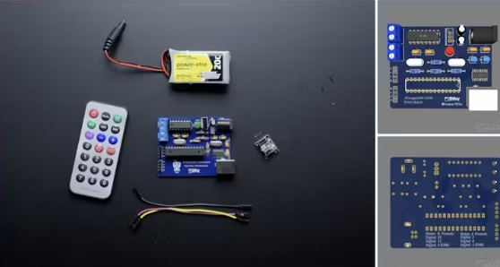
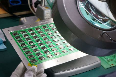
Automation in PCB Design and Assembly
Automation in PCB manufacturing has revolutionized how pcb manufacturing companies design and assemble Printed Circuit Boards (PCBs). By integrating automated systems, manufacturers can significantly reduce pcb manufacturing cost, increase production speed, and improve accuracy, leading to an overall enhancement in product quality. Automated machinery, such as pick-and-place robots and Surface Mount Technology (SMT) equipment, ensures that components are accurately placed and soldered, eliminating the possibility of human error. Furthermore, automated optical inspection (AOI) systems help detect defects early in the production process, ensuring higher reliability of the final product. Robotics and machinery allow pcb manufacturing businesses to scale quickly while maintaining consistent quality standards. These technologies not only speed up production but also make it more efficient by optimizing resource management through pre-programmed software tools that handle complex routing tasks with precision. As a result, pcb manufacturing has become more competitive and sustainable, setting new benchmarks for future innovations in electronics.
Cutting-Edge Software Tools for Efficient PCB Layout
In the fast-evolving landscape of pcb manufacturing, advanced software tools are revolutionizing how circuit boards are designed and produced. These tools offer pcb manufacturing companies powerful capabilities that significantly enhance design precision and efficiency. Today’s cutting-edge software applications utilize detailed simulations to test designs virtually, allowing you to spot and rectify errors before physical prototypes are manufactured, thereby reducing pcb manufacturing cost. Additionally, these tools automate many time-consuming tasks such as routing and component placement, enabling you to focus on more complex design elements and innovations. The integration of machine learning algorithms into these applications assists in predicting potential design issues, further streamlining the entire pcb manufacturing business process. Ultimately, adopting these advanced software solutions can lead to faster turnaround times, improved product reliability, and a more sustainable production environment for your future projects.
Sustainable Practices in PCB Manufacturing
As the demand for electronic devices continues to grow, so does the importance of sustainable practices in PCB manufacturing. Modern pcb manufacturing companies are increasingly adopting eco-friendly methods to reduce their environmental footprint. One of the major strategies includes the use of lead-free solder and halogen-free laminates, which minimize toxic waste. Additionally, many companies are implementing closed-loop recycling systems to reclaim and reuse raw materials, thereby significantly cutting down on pcb manufacturing cost and waste. Another emerging trend is the energy-efficient design of production facilities that aim to lower carbon emissions. By integrating renewable energy sources like solar and wind power into their operations, these companies not only contribute positively to the environment but also improve their overall efficiency and cost-effectiveness. Emphasizing sustainable practices is not just good for the planet; it also presents a lucrative opportunity for businesses in the pcb manufacturing business as consumers become more environmentally conscious. Therefore, embracing sustainability is essential for shaping a greener and more efficient future in PCB manufacturing.
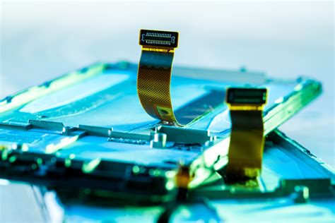
Enhancing Product Reliability through Innovative Materials
Achieving high product reliability is paramount in pcb manufacturing, where innovative materials play a crucial role. By incorporating materials such as flexible substrates and advanced laminates, pcb manufacturing companies are significantly enhancing the durability and performance of electronic devices. High-temperature resistant substrates and low-loss dielectric materials are particularly advantageous in producing boards that can withstand severe conditions while maintaining signal integrity. Additionally, advancements in bio-based and recyclable materials not only increase the longevity of the PCBs but also cater to the growing demand for environmentally friendly solutions. Utilizing these state-of-the-art materials notably contributes to decreased pcb manufacturing cost by reducing waste and improving efficiency, ultimately benefiting the entire pcb manufacturing business. This integration of innovative materials ensures that your products not only meet but exceed quality and reliability standards, paving the way for cutting-edge electronic solutions.
The Future Impact of Evolving PCB Technologies on Electronics
As PCB manufacturing continues to evolve, the future of electronics is poised for groundbreaking advancements. Cutting-edge techniques like High-Density Interconnect (HDI) technology and 3D printing are revolutionizing the way PCB manufacturing companies design and produce circuits. These advancements are not only enhancing design efficiency but also significantly boosting product reliability. Additionally, the integration of automation in pcb manufacturing has streamlined the production process, reducing both time and pcb manufacturing cost, thus making it feasible for smaller pcb manufacturing business ventures to thrive. Moreover, cutting-edge software tools are playing a crucial role in optimizing PCB layouts, making the entire operation more efficient. The incorporation of sustainable practices is also a noteworthy trend, ensuring that future technologies are not just advanced but also environmentally friendly. This ongoing transformation underscores the pivotal role of innovative PCB technologies in shaping the next generation of electronic devices, making them more reliable and cost-effective for consumers around the globe.
Conclusion
In summary, the evolution of PCB manufacturing is poised to revolutionize the electronics industry. With the integration of high-density interconnect (HDI) technology, 3D printing methods, and automation, PCB manufacturing companies are achieving unprecedented levels of efficiency and reliability. Cutting-edge software tools are streamlining designs, ensuring rapid prototyping and reducing PCB manufacturing cost. Moreover, sustainable practices are becoming a cornerstone of the PCB manufacturing business, aligning environmental concerns with industrial advancement. By embracing these technological innovations, the future landscape of electronics is set to become more dynamic and sustainable. To explore more about these advancements, you can visit Andwin PCBA.
Frequently Asked Questions
When it comes to PCB manufacturing, you might have several questions about the processes, technologies, and costs involved. Here are some common queries answered for your convenience:
1. What is PCB manufacturing?
PCB manufacturing refers to the process of designing and producing printed circuit boards. These boards are essential components that connect electronic components through conductive pathways.
2. How is HDI technology changing PCB manufacturing?
High-Density Interconnect (HDI) technology allows for more circuitry to be packed into smaller spaces. This leads to more efficient and compact electronic devices, making HDI a game-changer for many PCB manufacturing companies.
3. What role does 3D printing play in PCB production?
The integration of 3D printing in PCB production has made it possible to create complex designs with greater precision and less waste, thereby reducing the overall pcb manufacturing cost.
4. How does automation influence PCB design and assembly?
Automation streamlines the entire production process, from design to assembly, making it faster and less prone to errors. This shift towards automation is helping pcb manufacturing businesses remain competitive and cost-efficient.
5. Are there any sustainable practices in PCB manufacturing?
Yes, many companies are adopting environmentally friendly practices by recycling materials and reducing waste during production. These sustainable methods not only help the planet but can also lower costs in the long run.
Discover More about Advanced PCB Manufacturing
For more details on advanced technologies enhancing pcb manufacturing, please click here.