Revolutionizing Electronics with Additive PCB Manufacturing
Key Takeaways
In today’s fast-paced electronics landscape, additive PCB manufacturing is paving the way for unprecedented advancements. As you delve into this innovative realm, it’s essential to recognize how this technology fundamentally transforms the PCB manufacturing process. The shift towards 3D-printed PCBs enables pcb manufacturing companies to craft intricate designs with unparalleled precision and speed. This not only leads to significant cost savings but also optimizes the overall pcb manufacturing cost by reducing material waste and streamlining production timelines. Furthermore, the flexibility afforded by additive techniques allows you to explore a broader spectrum of designs; you can push the boundaries of conventional circuit board layouts and functionality, enhancing your project’s potential. By adopting this modern approach in your pcb manufacturing business, you position yourself at the forefront of innovation, ready to embrace future trends that promise to further revolutionize how electronics are designed and produced.
Introduction to Additive PCB Manufacturing: An Overview
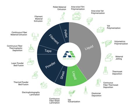
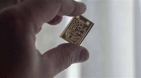
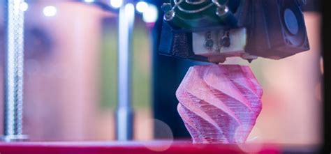
Additive PCB manufacturing is redefining the way electronics are developed, offering solutions that address some of the traditional hurdles associated with conventional PCB manufacturing methods. This innovative approach allows PCB manufacturing companies to create circuit boards layer by layer, utilizing materials efficiently and minimizing waste. By employing techniques such as 3D printing, designers and engineers can realize complex geometries that were previously impossible or extremely costly to achieve.
Table 1 below outlines some of the key features that differentiate additive manufacturing from traditional methods in PCB manufacturing:
| Feature | Traditional PCB Manufacturing | Additive PCB Manufacturing |
|---|---|---|
| Production Process | Subtractive | Additive |
| Material Waste | High | Low |
| Design Complexity | Limited | High |
| Lead Time for Prototyping | Longer | Shorter |
The advantages of this method are clear as it not only reduces the PCB manufacturing cost, but also accelerates the timeline for product development, giving businesses a competitive edge. As you explore options within this evolving field, consider how embracing additive techniques can transform your approach to your PCB manufacturing business, enhancing design flexibility and overall efficiency. The transformative potential of 3D-printed PCBs marks a significant advancement in modern electronics, paving the way for a new era of innovation in the industry. For more insights on this technology, check out the resources available through Andwin PCB.
The Advantages of 3D Printed PCBs in Electronics
In the ever-evolving field of electronics, 3D printed PCBs offer a range of advantages that are reshaping the landscape of PCB manufacturing. One significant benefit is the ability to drastically reduce the PCB manufacturing cost. Traditional methods often involve lengthy processes and substantial material waste, whereas additive techniques allow for more efficient use of resources, eliminating excess and leading to cost-effective solutions for PCB manufacturing companies. Additionally, you will find that the design flexibility provided by 3D printing enables you to experiment with complex geometries and unorthodox layouts that were previously impractical or impossible to achieve with standard techniques. This not only empowers you as a designer but also accelerates the development process within your PCB manufacturing business, making innovation more accessible than ever. Furthermore, with shorter production timelines, you can respond more quickly to market demands and technological trends, allowing your organization to maintain a competitive edge in an industry driven by rapid change. As you delve into additive PCB manufacturing, you’ll discover how these benefits can collectively transform your approach to electronics design and production.
Cost Savings and Efficiency Gains with Additive Techniques
Additive PCB manufacturing is reshaping the financial landscape for those involved in the electronics sector. By utilizing additive techniques, you can significantly reduce production costs associated with traditional methods. Unlike conventional PCB manufacturing companies that often incur high setup expenses and lengthy lead times, additive methods allow for seamless adjustments in design, leading to minimal waste and efficient resource allocation. This rapid prototyping capability not only elevates your ability to iterate designs but also substantially lowers the overall PCB manufacturing cost. Moreover, as you streamline your PCB manufacturing business, you position yourself to respond swiftly to market demands, enhancing both responsiveness and competitiveness. The shift towards additive approaches can thus foster a notable increase in operational efficiency while delivering substantial savings that directly impact your bottom line. This ongoing transformation highlights the myriad advantages that come with embracing innovative solutions in the realm of electronics production.
Design Flexibility: Pushing the Boundaries of PCB Innovation
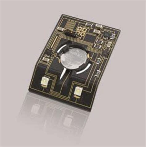
In the competitive world of pcb manufacturing, design flexibility is increasingly becoming a vital factor that differentiates successful projects. With traditional methods, constraints often limited how you could approach the layout and functionality of your printed circuit boards (PCBs). However, additive PCB manufacturing is opening new avenues for creativity and innovation. This technique allows you to explore intricate designs that would be prohibitively complex using conventional methods, such as multi-layered boards or embedded components. As you consider your options, remember that working with pcb manufacturing companies adopting additive techniques can significantly enhance your design possibilities.
Moreover, this innovative approach not only allows for more complex designs but also encourages rapid iterations. You can tweak designs on-the-fly without incurring substantial pcb manufacturing costs, making it easier to tailor products to specific market needs or customer requirements. The increased agility in design processes fosters an environment where prototyping can be accomplished in days rather than weeks. With reduced lead times and enhanced flexibility, you’ll find that evolving your product in response to feedback becomes much more practical.
“Embrace additive techniques as a game changer for your pcb manufacturing business,” suggests industry insider Laura Chen.
As these advancements continue to gain traction, the potential for improved product functionalities and innovative applications becomes limitless. This transformation encourages electronics developers to think outside the box and bring groundbreaking concepts from vision to reality with remarkable efficiency.
Speeding Up Production: How Additive Manufacturing Changes Timelines
In the fast-paced world of pcb manufacturing, staying ahead of production timelines is crucial. Additive PCB manufacturing has emerged as a game changer, allowing for rapid prototyping and shorter lead times. By leveraging advanced 3D-printing techniques, you can significantly reduce the time it takes to develop prototypes and move them into production. Unlike traditional methods employed by many pcb manufacturing companies, additive techniques enable you to create complex designs without the need for extensive tooling or setup, which can often be a bottleneck in the production process. This efficiency not only accelerates your timeline but also minimizes pcb manufacturing costs associated with lengthy setup and adjustments. As you explore these innovative technologies, consider how this shift in manufacturing approach can enhance your pcb manufacturing business. This newfound speed empowers you to respond swiftly to market demands, adapt designs in real time, and ultimately drive competitiveness in a landscape where demand for faster delivery times is ever-increasing. With additive methods paving the way for quicker turnarounds, you’re better equipped to keep pace with evolving customer expectations and technological advancements.
Case Studies: Successful Implementations of Additive PCB Manufacturing
Across various sectors, additive PCB manufacturing has demonstrated remarkable advantages, leading to innovative implementations that can serve as models for your own PCB manufacturing business. Companies like Intel and HP have embraced this technology, showcasing how 3D-printed PCBs can streamline processes and reduce PCB manufacturing cost. For instance, Intel applied additive techniques in developing its IoT devices, resulting in a reduction of prototype production times from weeks to mere days. In another case, HP utilized additive techniques to create complex designs that traditional methods could not accommodate. This leap in design flexibility has propelled these firms ahead of the curve while highlighting the capabilities of various PCB manufacturing companies. Such implementations illustrate not just efficiency gains but also how these companies are pushing the boundaries of electronics design. The real-world applications reflect a transformative shift in the industry, encouraging further exploration of the potential embodied in additive technologies for future projects. If you are considering entering or evolving within this space, these examples can provide invaluable insights into successful strategies and outcomes that await those willing to innovate in their own approaches to PCB manufacturing.
Future Trends in Additive PCB Technology and Its Impact on Electronics
As you look toward the future of additive PCB manufacturing, it’s essential to understand the profound impacts it will have on the electronics industry. The rise of 3D printed PCBs is not just a trend; it’s reshaping how PCB manufacturing companies approach design and production. You can expect significant advancements in materials that allow for greater functionality and performance. These innovations will reduce PCB manufacturing costs, making it possible for startups and established businesses alike to explore new possibilities without breaking the bank. Additionally, as you dive deeper into the evolving landscape, you’ll find that flexibility in design will enable more intricate and customized electronics, catering directly to specific user needs. This shift isn’t merely about efficiency; it represents a broader transformation in the way you think about electronics development. The ability to create prototypes quickly and iterate designs rapidly will not only accelerate your development timelines but also foster innovation within your PCB manufacturing business. With these exciting advancements, staying ahead of competitor offerings becomes paramount as the industry continues to evolve at an unprecedented pace.
Conclusion: The Transformative Power of Additive Manufacturing in the Industry
The rise of additive PCB manufacturing has markedly changed the landscape of the electronics sector, making it essential for those involved in the pcb manufacturing business to adapt and evolve. With pcb manufacturing companies embracing this transformative approach, you can expect a shift towards more efficient operations and reduced pcb manufacturing costs. The flexibility inherent in 3D-printed PCBs allows for innovative designs that were previously impractical, enabling you to push the boundaries of what is possible. This not only fosters creativity but also expedites production timelines, aligning with the increasing demand for faster turnaround. As a result, staying ahead of trends is crucial; by integrating additive techniques, you can leverage these advancements to create products that meet the dynamic needs of today’s market. In turn, this will position your pcb manufacturing business at the forefront of technological progress, enhancing your competitive edge in an ever-evolving industry.
Conclusion: The Transformative Power of Additive Manufacturing in the Industry
In the ever-evolving landscape of PCB manufacturing, additive techniques have emerged as a game-changer, profoundly influencing how PCB manufacturing companies approach design and production. The pcb manufacturing cost has significantly decreased, allowing businesses to allocate resources more effectively while maintaining quality. This transformation is particularly beneficial for startups and established pcb manufacturing businesses alike, providing them with the agility to innovate without the constraints traditionally imposed by conventional methods. With the adoption of 3D-printed PCBs, you can significantly enhance design flexibility, enabling you to create complex geometries and integrate multiple functions into a single board. This innovative approach not only accelerates your production timelines but also enhances your capability to respond to market changes with greater speed and efficiency. As you explore the potential of additive PCB manufacturing, you’ll witness how these advancements not only streamline operations but also pave the way for cutting-edge electronics solutions tailored to meet contemporary demands.
FAQs
What is additive PCB manufacturing?
Additive PCB manufacturing refers to the process of creating printed circuit boards (PCBs) using additive techniques, such as 3D printing. This method allows for the layer-by-layer construction of circuits, contrasting with traditional subtractive methods.
How does additive manufacturing affect PCB manufacturing cost?
With additive PCB manufacturing, you may experience lower PCB manufacturing costs due to reduced material waste and shorter production times. This efficiency often translates into significant savings for PCB manufacturing companies.
What advantages do additive techniques offer over traditional methods?
Additive techniques provide enhanced design flexibility, enabling you to create complex geometries that traditional PCB manufacturing businesses struggle with. These methods allow for rapid prototyping and modifications, making it easier to innovate.
Can you provide examples of successful implementations in the industry?
Numerous leading PCB manufacturing companies have successfully integrated additive processes. These case studies demonstrate how companies have achieved quicker turnaround times and more cost-effective production through advanced technologies.
What are the future trends in additive PCB technology?
Future trends indicate a surge in the adoption of additive PCB manufacturing, driven by ongoing innovations that focus on enhancing efficiency and scalability. Expect to see more industries leveraging this technology for bespoke solutions.


