Revolutionizing Technology: The Art and Science of Printed Circuit Board Assembly
Key Takeaways
Understanding the world of printed circuit boards (PCBs) is essential, as these components serve as the backbone of modern electronics. The process of pcb assembly, or PCBA, involves intricate designs that must harmonize both aesthetic elements and functional requirements. Key innovations in this field include automated manufacturing processes and advanced robotics, which significantly enhance precision and efficiency in the pcb assembly process. Sustainability has also become a priority, with manufacturers adopting eco-friendly practices that not only reduce waste but also improve production reliability. Collaboration among industry leaders is pushing the boundaries of what is possible in PCB technology, leading to new standards and innovations that keep pace with rapidly evolving electronic demands. Observing these trends provides valuable insights into how they will shape the future of electronic manufacturing, ensuring that pcba remains a critical focus as we advance into an increasingly digital world.
Understanding Printed Circuit Boards: The Backbone of Modern Electronics
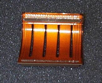
Printed Circuit Boards, or PCBs, serve as the fundamental building blocks of modern electronics, providing the necessary framework for electrical connections and component placement. The assembly of printed circuit boards is an intricate process that combines a variety of components into a cohesive unit, enabling devices to function effectively. Each PCB assembly (or PCBA) is meticulously designed to maximize efficiency, reliability, and performance.
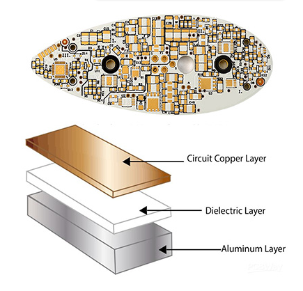
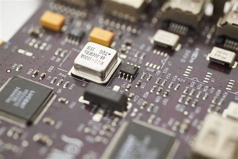
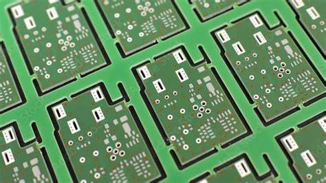
At its core, a PCB consists of a non-conductive substrate that hosts conductive pathways, usually made from copper, connecting the various electronic components such as resistors and capacitors. The assembly process involves several stages including soldering components to the board, testing for faults, and ensuring that all connections meet the required specifications. Innovative techniques such as surface-mount technology (SMT) have revolutionized this process, allowing for smaller and more complex designs.
The importance of sustainable practices in PCB assembly cannot be overlooked either. As the demand for electronics continues to grow, companies are increasingly adopting environmentally friendly materials and processes to reduce waste and improve recyclability. This shift not only benefits the planet but also enhances brand reputation among environmentally conscious consumers.
Moreover, collaborative efforts among industry stakeholders are driving advancements in PCB manufacturing techniques. From research institutions to technology companies, partnerships are helping to develop cutting-edge solutions that propel the future of electronic manufacturing. As we advance further into an age dominated by digital technology, understanding the significance of PCBs will be crucial in navigating and shaping tomorrow’s electronic landscape.
| Component Type | Function |
|---|---|
| Resistors | Limit current flow |
| Capacitors | Store electrical energy |
| Integrated Circuits | Combine multiple functions into one unit |
| Connectors | Allow connections between different boards |
In summary, understanding PCBs reveals their essential role in modern electronics as they provide both structure and connectivity while embodying innovations that pave the way for technological advancement.
The Art of PCB Design: Balancing Aesthetics and Functionality
The design of printed circuit boards (PCBs) encompasses a delicate interplay between aesthetics and functionality. Successful pcb assembly not only fulfills technical requirements but also presents a visual harmony that reflects the ethos of the device it serves. Designers must carefully consider component placement, trace routing, and overall layout to ensure that the final product is both efficient and appealing. A well-executed PCB design minimizes electrical noise, improves signal integrity, and facilitates easier assembly processes while presenting a visually organized structure that can be appreciated in both etching and final form. Advanced software tools play a pivotal role in achieving this balance, enabling designers to simulate performance under various conditions before physical production begins. By leveraging these technologies, designers can create pcba solutions that enhance usability and promote brand identity without sacrificing the robustness necessary for reliable performance. This harmonious blend is not merely an aesthetic choice; it is vital for meeting consumer expectations in an increasingly competitive market, where functionality must seamlessly integrate with visual appeal to drive innovation in electronic manufacturing.
Scientific Innovations in PCB Assembly Techniques
The field of pcb assembly is witnessing rapid transformation thanks to groundbreaking scientific innovations. These advancements are pivotal in achieving higher precision and efficiency in the assembly process of printed circuit boards (PCBs). One of the most notable innovations is the development of advanced soldering techniques, which enhance the reliability and longevity of pcba components. Moreover, cutting-edge materials are now being used, such as low-temperature solder alloys that not only reduce thermal stress on sensitive components but also improve overall manufacturing sustainability.
Furthermore, technologies like automated optical inspection (AOI) play a crucial role in ensuring quality control throughout the assembly process. By utilizing machine learning algorithms, these inspections can identify potential defects at a considerably faster rate than human inspection could achieve. This level of oversight significantly minimizes errors, thereby leading to less wastage and reducing costs associated with rework.
“Embracing innovative techniques in PCB assembly isn’t just about keeping pace with technology; it’s about setting new standards for quality and efficiency.”
Collaboration between engineers and software developers has also resulted in sophisticated design tools that streamline the pcb assembly workflow. These tools allow for real-time simulations and adjustments based on predicted performance, enhancing both design efficiency and manufacturability.
Overall, these scientific innovations are not merely incremental improvements; they represent a fundamental shift in how electronic manufacturing operates, enabling companies to meet the growing demands for faster production times without compromising quality. As these technologies continue to evolve, they will undoubtedly shape the future landscape of pcba, fueling advancements that will power an increasingly complex digital world.
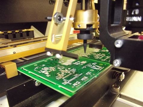
Enhancing Efficiency: Automation and Robotics in PCB Assembly
The landscape of pcb assembly is rapidly evolving, with automation and robotics playing pivotal roles in enhancing productivity and precision. In modern pcba processes, automated systems have been integrated to manage repetitive tasks such as component placement, soldering, and inspection. This technological advancement not only accelerates production speed but also significantly reduces the likelihood of human error, leading to higher-quality outputs. Moreover, the integration of robotics allows for consistent performance across various production runs, making it easier to maintain tight tolerances essential in today’s intricate electronic designs. The synergy of these technologies fosters an environment where innovations can flourish—promoting sustainability through reduced waste and more efficient resource use. As manufacturers increasingly adopt automated solutions, they are transforming the methods employed in pcb assembly, driving the industry toward a future defined by agility and responsiveness to market demands. By embracing automation and robotics, the potential for enhancing overall operational efficiency becomes clearer, ultimately shaping a more robust electronic manufacturing ecosystem that meets the evolving needs of our digital age.
Sustainable Practices in Printed Circuit Board Production
Sustainability in pcb assembly has become a pivotal concern for manufacturers striving to reduce their environmental impact while maintaining efficiency and effectiveness. The journey toward greener practices begins with the selection of materials. Printed circuit boards (PCBs) can be produced using eco-friendly substances, such as lead-free solder and recyclable substrates, which minimize hazardous waste and support the circular economy. Additionally, advancements in technology allow manufacturers to employ efficient energy practices—including renewable energy sources within production facilities—that lessen reliance on fossil fuels. The integration of automation further enhances sustainability efforts by reducing material waste through precise manufacturing processes. Moreover, leading organizations are investing in workforce training to promote awareness of sustainable methods within the industry, ensuring that all employees contribute to reducing ecological footprints during the pcba process. By prioritizing sustainability, manufacturers not only fulfill regulatory requirements but also appeal to a growing market of environmentally-conscious consumers, positioning themselves favorably for future growth while playing a vital role in preserving our planet.
Collaborative Efforts in Advancing PCB Manufacturing
In the realm of printed circuit board assembly (PCBA), collaboration among various stakeholders is essential for driving innovation and improving processes. Manufacturers, designers, and technology providers increasingly recognize that pooling their expertise can lead to significant advancements. For instance, a partnership between software developers and PCB fabricators can enhance design accuracy through sophisticated simulation tools that foresee potential issues before physical assembly occurs. Additionally, the integration of automation and robotics in PCB assembly not only streamlines production but also minimizes human error, thereby increasing overall efficiency. Companies that engage in collaborative research projects often share best practices and insights into sustainable manufacturing processes, which pave the way for greener alternatives in the industry. Furthermore, these joint efforts extend to educational institutions where knowledge transfer fosters a new generation of skilled workers adept in cutting-edge techniques for printed circuit boards. In this dynamic environment, active collaboration is not just beneficial; it is essential for maintaining competitiveness and fostering innovation within the ever-evolving landscape of electronic manufacturing.
The Future of Electronics: Trends Shaping PCB Technology
The landscape of pcb assembly is undergoing a transformative shift, driven by several compelling trends that are redefining the future of electronics. One key trend is the integration of smart technologies, where the Internet of Things (IoT) and artificial intelligence are enabling more efficient and intelligent pcba processes. Manufacturers are adopting advanced data analytics to optimize production lines, improving both speed and accuracy in pcb assembly. Additionally, miniaturization remains a powerful trend, with components becoming smaller and more densely packed on circuit boards while maintaining performance standards. This requires innovative design strategies that push the boundaries of traditional pcb assembly methods.
Moreover, sustainability is now at the forefront of production considerations. Companies are increasingly focusing on eco-friendly materials and waste reduction practices to minimize their environmental footprint during the pcba process. This shift is not only beneficial for the planet but also meets rising consumer demand for responsible manufacturing.
Collaboration across industries is also playing a pivotal role in advancing pcb assembly technology. Partnerships between tech companies, academic institutions, and manufacturers foster knowledge exchange and spur innovative solutions to complex challenges faced in this field. As these trends converge, they promise to propel the future of electronics into an era characterized by enhanced functionality, efficiency, and sustainability in pcb assembly, ultimately transforming how we interact with technology in our daily lives.
Case Studies: Successful Implementations of Advanced PCB Assembly Techniques
The evolution of pcb assembly has been marked by numerous case studies that illustrate the successful implementation of advanced techniques across various industries. For instance, a leading telecommunications company recently adopted state-of-the-art pcba technology that streamlined its production process. By integrating automation and robotics into its assembly lines, the company achieved a remarkable increase in throughput while maintaining high levels of accuracy. This shift not only minimized errors but also reduced waste, showcasing a sustainable approach to modern pcb assembly practices. Furthermore, in a groundbreaking partnership between a tech startup and an established electronics firm, novel algorithms designed to optimize routing and placement were introduced. This collaboration resulted in the accelerated development of compact, high-performance devices that exemplify the intricate balance between aesthetics and functionality inherent in effective pcba design. Such successful implementations highlight how innovative strategies are not only transforming manufacturing processes but also setting new benchmarks for quality and sustainability in the electronic industry. As these case studies illustrate, advancing pcb assembly techniques is pivotal for staying competitive in an ever-evolving technological landscape.
Conclusion
In summary, the pcb assembly process stands as a cornerstone of electronic manufacturing, merging both artistic vision and scientific precision. As we have discovered throughout this article, the advancements in pcba techniques have revolutionized how we approach the assembly of printed circuit boards. Innovations in automation and robotics are dramatically enhancing efficiency while also reducing human error—making each assembly not just faster but also more reliable. Furthermore, the focus on sustainability and eco-friendly practices in pcb production reflects a growing awareness of environmental responsibilities within the industry. The collaborative efforts between manufacturers, designers, and technologists are driving continuous improvement, ensuring that pcb assembly not only meets current demands but anticipates future needs. As we look to the future of electronics, it is clear that these developments in pcba will play an essential role in shaping how devices are designed and function in our increasingly digital world.
FAQs
The assembly of printed circuit boards, commonly referred to as PCB assembly or PCBA, is an intricate process that involves various stages and technologies. Many individuals may wonder about the specific steps involved in this critical operation. First and foremost, it is essential to understand that PCB assembly begins with the design and layout of the circuit board itself, which serves as the base for all electronic components. Once the design is finalized, the next phase includes applying solder paste onto designated pads, followed by placing components accurately on the board using automated pick-and-place machines.
Furthermore, many people inquire about the role of automation in PCBA. Modern advancements have introduced significant improvements in automation techniques that enhance both efficiency and precision throughout the PCB assembly process. Automated soldering methods have replaced traditional hand soldering to ensure consistency and reduce errors.
Sustainability is another common concern related to printed circuit board production. As industries prioritize eco-friendly practices, innovations in materials and recycling methods are being integrated into PCB manufacturing. This not only helps reduce waste but also promotes responsible sourcing of materials which is increasingly important in today’s manufacturing landscape.
When it comes to troubleshooting and maintaining quality during PCB assembly, many professionals emphasize the importance of regular testing at various stages of production. Techniques such as Automated Optical Inspection (AOI) are utilized to ensure that every component is placed correctly and that there are no defects that could compromise functionality.
If you have additional questions or would like to dive deeper into this fascinating topic, please click here: Andwin PCB Assembly for more information!