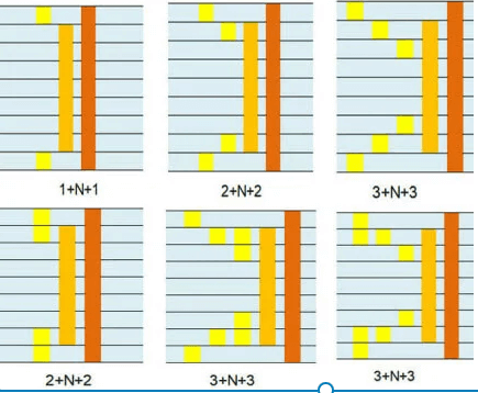
Rf attenuator pcb
Design Considerations For RF Attenuator PCBs
Designing RF attenuator PCBs requires meticulous attention to detail and a comprehensive understanding of both electrical and mechanical considerations. The primary objective is to ensure that the attenuator performs its function of reducing signal strength without introducing significant distortion or noise. To achieve this, several key factors must be taken into account during the design process.
Firstly, the choice of materials is paramount.
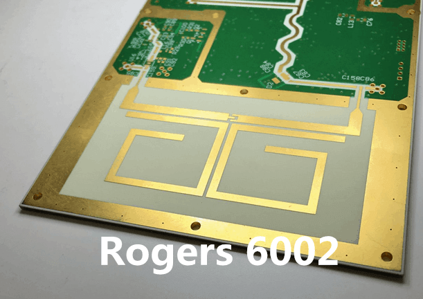
High-frequency signals are particularly susceptible to losses and interference, so selecting a substrate with low dielectric loss is essential. Materials such as Rogers or Teflon-based laminates are often preferred due to their superior performance at high frequencies. Additionally, the thickness of the substrate can influence the impedance of the transmission lines, necessitating precise calculations to maintain signal integrity.
Transitioning to the layout of the PCB, the placement of components is critical.
RF attenuators typically consist of resistive elements arranged in specific configurations, such as Pi or T networks. These components must be placed in close proximity to minimize parasitic inductance and capacitance, which can degrade performance. Furthermore, the layout should ensure that the signal path is as short and direct as possible, reducing the potential for signal degradation.
Another important consideration is the grounding strategy.
A solid and continuous ground plane is essential for maintaining signal integrity and minimizing electromagnetic interference (EMI). The ground plane acts as a reference point for the signal and helps to shield sensitive components from external noise. Careful attention must be paid to the placement of vias and the routing of ground connections to ensure a low-impedance path to ground.
Thermal management is also a crucial aspect of RF attenuator PCB design.
Attenuators can dissipate significant amounts of power, leading to heat generation that can affect performance and reliability. Effective thermal management strategies, such as the use of thermal vias, heat sinks, and appropriate copper thickness, are necessary to dissipate heat efficiently and maintain stable operation.
In addition to these electrical and thermal considerations, mechanical factors must also be addressed.
The physical size and shape of the PCB can impact its performance, particularly at higher frequencies. Ensuring that the PCB is rigid and free from mechanical stress can help to maintain consistent electrical characteristics. Moreover, the choice of connectors and their placement can influence the overall performance of the attenuator. High-quality RF connectors with low insertion loss and good impedance matching are essential for minimizing signal reflections and losses.
Testing and validation are integral parts of the design process.
Once the PCB is fabricated, it must be thoroughly tested to ensure that it meets the desired specifications. This involves measuring parameters such as insertion loss, return loss, and attenuation accuracy across the intended frequency range. Any discrepancies must be addressed through iterative design adjustments and re-testing.
In conclusion, designing RF attenuator PCBs involves a careful balance of material selection, component placement, grounding strategies, thermal management, and mechanical considerations. Each of these factors plays a crucial role in ensuring that the attenuator performs its intended function effectively and reliably. By paying close attention to these design considerations, engineers can create high-performance RF attenuators that meet the stringent demands of modern communication systems.
Common Applications Of RF Attenuator PCBs
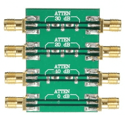
RF attenuator PCBs, or printed circuit boards, play a crucial role in various applications within the realm of radio frequency (RF) technology. These components are designed to reduce the power of a signal without significantly degrading its quality, making them indispensable in numerous fields. Understanding the common applications of RF attenuator PCBs can provide insight into their importance and versatility in modern technology.
One of the primary applications of RF attenuator PCBs is in telecommunications.
In this sector, maintaining signal integrity is paramount, and RF attenuators help achieve this by managing signal levels. For instance, in cellular networks, RF attenuators are used to balance signal strength between different cells, ensuring that communication remains clear and reliable. By preventing signal overload, they help maintain the quality of voice and data transmission, which is critical for both personal and commercial communication.
Moreover, RF attenuator PCBs are extensively used in test and measurement equipment.
Engineers and technicians rely on precise measurements to develop and maintain RF systems, and attenuators are essential in this process. They allow for the calibration of instruments by providing known levels of signal attenuation, which is crucial for accurate testing. This application is particularly important in the development of new RF technologies, where precise measurements can mean the difference between success and failure.
In addition to telecommunications and testing, RF attenuator PCBs find applications in broadcasting.
Television and radio stations use these components to control signal levels, ensuring that broadcasts reach their intended audience without interference or distortion. By managing the power of transmitted signals, RF attenuators help maintain the quality and consistency of broadcasts, which is essential for both public and commercial broadcasting services.
Furthermore, RF attenuator PCBs are vital in satellite communication systems.
Satellites operate in a complex environment where signal strength can vary significantly. Attenuators help manage these variations, ensuring that signals are transmitted and received at optimal levels. This is particularly important for maintaining the reliability of satellite-based services, such as GPS, weather forecasting, and global communications.
Another significant application of RF attenuator PCBs is in military and aerospace technology.
In these fields, the reliability and precision of communication systems are of utmost importance. RF attenuators help manage signal levels in radar systems, communication devices, and electronic warfare equipment. By ensuring that signals are transmitted and received at appropriate levels, they contribute to the effectiveness and safety of military operations.
Additionally, RF attenuator PCBs are used in consumer electronics.
Devices such as smartphones, Wi-Fi routers, and Bluetooth-enabled gadgets all rely on RF technology. Attenuators help manage signal strength in these devices, ensuring that they operate efficiently and without interference. This application highlights the ubiquity of RF attenuators in everyday life, as they contribute to the seamless functioning of various electronic devices.
In conclusion, RF attenuator PCBs are integral to a wide range of applications, from telecommunications and broadcasting to satellite communication and military technology. Their ability to manage signal levels without compromising quality makes them indispensable in ensuring the reliability and efficiency of RF systems. As technology continues to advance, the importance of RF attenuator PCBs is likely to grow, underscoring their critical role in modern communication and electronic systems.
Material Selection For RF Attenuator PCB Fabrication
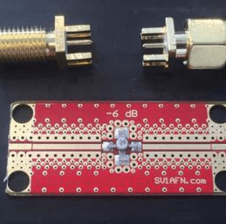
When designing an RF attenuator PCB, the selection of materials is a critical factor that significantly influences the performance, reliability, and longevity of the final product. The choice of substrate, conductive materials, and dielectric properties must be meticulously considered to ensure optimal functionality in high-frequency applications. To begin with, the substrate material forms the foundation of the PCB and plays a pivotal role in determining its electrical and thermal characteristics. For RF applications, materials such as Rogers RT/duroid, Taconic, and Arlon are often preferred due to their low dielectric constant and minimal loss tangent. These properties are essential for maintaining signal integrity and minimizing signal loss, which are crucial in RF circuits.
In addition to the substrate, the conductive materials used for the traces and pads are equally important.
Copper is the most commonly used conductive material due to its excellent electrical conductivity and relatively low cost. However, for high-frequency applications, the surface roughness of the copper can impact signal performance. Therefore, smooth copper or rolled copper is often used to reduce signal attenuation and improve overall performance. Furthermore, the thickness of the copper layer must be carefully selected to balance between current-carrying capacity and signal integrity.
The dielectric properties of the materials used in the PCB also play a significant role in the performance of an RF attenuator.
The dielectric constant (Dk) and dissipation factor (Df) are two critical parameters that must be considered. A low dielectric constant is preferred as it reduces signal propagation delay and minimizes signal loss. Similarly, a low dissipation factor is essential to reduce energy loss in the form of heat, which can degrade the performance of the RF attenuator over time. Materials such as PTFE (Polytetrafluoroethylene) and ceramic-filled laminates are often chosen for their superior dielectric properties.
Thermal management is another crucial aspect of material selection for RF attenuator PCBs.
High-frequency signals can generate significant amounts of heat, which can affect the performance and reliability of the PCB. Therefore, materials with good thermal conductivity are essential to dissipate heat effectively. Thermal vias and heat sinks can also be incorporated into the design to enhance thermal management. Additionally, the coefficient of thermal expansion (CTE) of the materials must be compatible with the components used to prevent mechanical stress and potential failure during thermal cycling.
Moreover, the environmental stability of the materials must be considered, especially for applications in harsh environments.
Materials that are resistant to moisture absorption, chemical exposure, and temperature variations are preferred to ensure long-term reliability. For instance, materials like Rogers RO4000 series and Isola FR408HR are known for their excellent environmental stability and are commonly used in RF applications.
In conclusion, the selection of materials for RF attenuator PCB fabrication is a complex process that requires careful consideration of various electrical, thermal, and environmental factors. By choosing the appropriate substrate, conductive materials, and dielectric properties, designers can ensure that the RF attenuator PCB performs optimally in high-frequency applications. The integration of thermal management solutions and consideration of environmental stability further enhance the reliability and longevity of the final product. Therefore, a thorough understanding of material properties and their impact on RF performance is essential for the successful design and fabrication of RF attenuator PCBs.
Troubleshooting Issues In RF Attenuator PCB Circuits
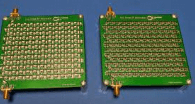
When troubleshooting issues in RF attenuator PCB circuits, it is essential to approach the task methodically to ensure accurate diagnosis and effective resolution. RF attenuators are critical components in various electronic systems, designed to reduce signal strength without significantly distorting the waveform. However, issues can arise due to a multitude of factors, including design flaws, component failures, and environmental influences. Understanding these potential problems and their solutions is key to maintaining optimal performance.
One of the primary issues encountered in RF attenuator PCB circuits is impedance mismatch.
Impedance matching is crucial in RF circuits to ensure maximum power transfer and minimize signal reflection. An impedance mismatch can lead to signal loss, distortion, and reduced efficiency. To address this, it is important to verify that the impedance of the attenuator matches the impedance of the source and load. This can be achieved by using a network analyzer to measure the impedance and make necessary adjustments to the circuit design or component values.
Another common problem is the presence of unwanted parasitic elements.
Parasitic capacitance and inductance can significantly affect the performance of RF attenuators, leading to signal degradation and instability. These parasitic elements often arise from poor PCB layout practices, such as inadequate spacing between traces or improper grounding. To mitigate these issues, it is advisable to follow best practices in PCB design, such as maintaining proper trace width and spacing, using ground planes, and minimizing the length of signal paths. Additionally, employing high-frequency simulation tools can help identify and address potential parasitic effects during the design phase.
Component selection also plays a vital role in the performance of RF attenuator circuits.
Using components with inadequate frequency response or poor tolerance can result in suboptimal performance. It is essential to choose components that are specifically designed for RF applications and have the necessary specifications to handle the desired frequency range. Furthermore, ensuring that components are properly rated for the operating conditions, such as temperature and power levels, can prevent premature failures and maintain circuit reliability.
Environmental factors, such as temperature variations and electromagnetic interference (EMI), can also impact the performance of RF attenuator PCB circuits.
Temperature changes can cause components to drift from their specified values, leading to variations in attenuation levels. To mitigate this, it is important to use temperature-stable components and consider thermal management techniques, such as heat sinks or thermal vias, to dissipate excess heat. EMI can introduce noise and interfere with the signal, degrading the performance of the attenuator. Shielding the circuit and using proper filtering techniques can help reduce the impact of EMI.
In addition to these technical considerations, thorough testing and validation are crucial in troubleshooting RF attenuator PCB circuits. Using tools such as spectrum analyzers, network analyzers, and oscilloscopes can provide valuable insights into the circuit’s performance and help identify any anomalies. Conducting tests under various operating conditions and comparing the results with the expected performance can aid in pinpointing the root cause of issues.
In conclusion, troubleshooting issues in RF attenuator PCB circuits requires a comprehensive understanding of the potential problems and their solutions. By addressing impedance mismatches, minimizing parasitic elements, selecting appropriate components, and considering environmental factors, one can effectively diagnose and resolve issues. Employing best practices in PCB design and thorough testing further ensures the reliability and optimal performance of RF attenuator circuits.

