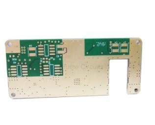
Rf circuit pcb design
Key Considerations For RF Circuit PCB Layout
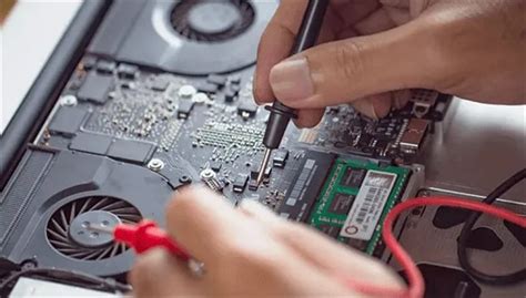
Designing a printed circuit board (PCB) for radio frequency (RF) circuits requires meticulous attention to detail and a deep understanding of both the electrical and physical properties of the components involved.
The performance of RF circuits is highly sensitive to layout, and even minor deviations can lead to significant issues such as signal loss, interference, and impedance mismatches. Therefore, several key considerations must be taken into account to ensure optimal functionality and reliability.
Firstly, the choice of materials is paramount.
High-frequency signals are particularly susceptible to losses caused by the dielectric properties of the PCB substrate. Materials such as FR-4, commonly used in standard PCBs, may not always be suitable for RF applications due to their higher dielectric losses at high frequencies. Instead, specialized low-loss materials like Rogers or Teflon-based substrates are often preferred. These materials offer better performance by minimizing signal attenuation and maintaining signal integrity over longer distances.
Transitioning to the layout itself, the placement of components is critical.
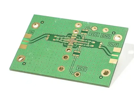
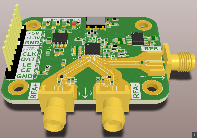
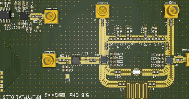
RF components should be placed as close to each other as possible to minimize the length of signal paths. This reduces the potential for signal degradation and electromagnetic interference (EMI). Additionally, the orientation of components can affect the coupling between them. Proper alignment can help mitigate unwanted interactions and improve overall circuit performance.
Another crucial aspect is the management of impedance.
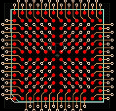
Impedance matching is essential to ensure maximum power transfer and minimize reflections in RF circuits. This involves carefully designing transmission lines, such as microstrip or stripline, with controlled impedance. The width of these lines, the spacing between them, and the properties of the substrate all play a role in determining the characteristic impedance. Tools like impedance calculators and simulation software can aid in achieving the desired impedance values.
Grounding is another vital consideration in RF PCB design.
A solid and continuous ground plane is necessary to provide a low-impedance return path for signals and to shield sensitive components from EMI. Ground planes should be as unbroken as possible, and multiple vias should be used to connect different layers of the PCB to the ground plane. This helps in reducing ground loops and maintaining signal integrity.
Thermal management also cannot be overlooked.
RF components, especially power amplifiers, can generate significant amounts of heat. Effective thermal management strategies, such as the use of thermal vias, heat sinks, and proper airflow, are essential to prevent overheating and ensure the longevity of the components.
Moreover, the use of decoupling capacitors is essential to filter out noise and stabilize the power supply.
These capacitors should be placed as close as possible to the power pins of active components to be effective. The values and types of capacitors used should be chosen based on the frequency range of the RF signals.
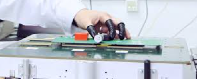
Finally, simulation and testing are indispensable steps in the RF PCB design process.
Simulation tools can help predict the behavior of the circuit and identify potential issues before the physical prototype is built. Once the PCB is fabricated, thorough testing using network analyzers, spectrum analyzers, and other RF measurement equipment is necessary to validate the design and ensure it meets the required specifications.
In conclusion, designing an RF circuit PCB involves a complex interplay of material selection, component placement, impedance management, grounding, thermal management, and thorough testing. By carefully considering these factors, designers can create high-performance RF circuits that meet the stringent demands of modern communication systems.
Techniques For Minimizing Signal Loss In RF PCB Design
In the realm of RF circuit PCB design, minimizing signal loss is paramount to ensuring optimal performance and reliability. Signal loss, often referred to as attenuation, can significantly degrade the functionality of RF circuits, leading to inefficiencies and potential failures. To address this, several techniques can be employed, each contributing to the overall integrity of the signal as it traverses the PCB.
One of the primary techniques for minimizing signal loss is the careful selection of materials.
The dielectric constant and loss tangent of the substrate material play crucial roles in determining the extent of signal attenuation. Low-loss materials, such as Rogers or Teflon-based substrates, are often preferred over traditional FR-4 due to their superior electrical properties. These materials exhibit lower dielectric losses, thereby preserving signal strength over longer distances.
In addition to material selection, the design of transmission lines is critical.
Microstrip and stripline configurations are commonly used in RF PCB design, each with its own set of advantages. Microstrip lines, which consist of a conductive trace on the surface of the PCB with a ground plane beneath, are easier to fabricate and inspect. However, they are more susceptible to radiation losses. Striplines, on the other hand, are sandwiched between two ground planes, offering better shielding and reduced radiation losses. The choice between these configurations depends on the specific requirements of the application.
Furthermore, impedance matching is essential to minimize signal reflection and loss.
Mismatched impedances between components and transmission lines can lead to significant signal degradation. To achieve proper impedance matching, designers often employ techniques such as the use of matching networks, which can include components like capacitors, inductors, and transformers. These networks are designed to ensure that the impedance of the source, transmission line, and load are all aligned, thereby minimizing reflections and maximizing power transfer.
Another technique involves the careful routing of traces.
The length and width of traces, as well as their proximity to other conductive elements, can impact signal integrity. To mitigate signal loss, designers should aim to keep trace lengths as short as possible and avoid sharp bends, which can introduce inductive and capacitive effects. Additionally, maintaining consistent trace widths and using controlled impedance routing can help preserve signal quality.
Grounding and shielding also play pivotal roles in minimizing signal loss.
A well-designed ground plane can provide a low-impedance return path for signals, reducing the potential for ground loops and noise. In high-frequency designs, it is often beneficial to use multiple ground planes or a solid ground plane to ensure a stable reference. Shielding techniques, such as the use of metal enclosures or ground vias, can further protect sensitive signals from external interference and crosstalk.
Moreover, the use of vias should be carefully considered. While vias are necessary for connecting different layers of a PCB, they can introduce parasitic inductance and capacitance, leading to signal degradation. Minimizing the number of vias and optimizing their placement can help reduce these parasitic effects. When vias are unavoidable, techniques such as back-drilling can be employed to remove unused portions of the via, thereby reducing their impact on signal integrity.
In conclusion, minimizing signal loss in RF PCB design requires a multifaceted approach that encompasses material selection, transmission line design, impedance matching, trace routing, grounding, shielding, and via optimization. By meticulously addressing each of these aspects, designers can significantly enhance the performance and reliability of RF circuits, ensuring that signals are transmitted with minimal attenuation and maximum fidelity.

Best Practices For RF PCB Material Selection
Selecting the appropriate material for RF PCB design is a critical step that significantly influences the performance, reliability, and manufacturability of the final product. The choice of material impacts various parameters such as signal integrity, thermal management, and overall system efficiency. Therefore, understanding the best practices for RF PCB material selection is essential for engineers and designers aiming to optimize their designs.
To begin with, one must consider the dielectric constant (Dk) of the material.
The dielectric constant affects the signal speed and impedance of the transmission lines. Materials with a low and stable Dk are preferred for high-frequency applications because they minimize signal loss and ensure consistent performance across different operating conditions. For instance, PTFE (Polytetrafluoroethylene) and ceramic-filled laminates are commonly used in RF applications due to their low Dk values and excellent electrical properties.
In addition to the dielectric constant, the dissipation factor (Df) is another crucial parameter.
The dissipation factor measures the dielectric losses within the material, which directly impacts signal attenuation. Lower Df values are desirable as they indicate reduced energy loss and better signal integrity. Materials such as Rogers RO3000 series and Taconic RF-35 are known for their low dissipation factors, making them suitable choices for high-frequency circuits.
Thermal management is another vital consideration in RF PCB material selection.
High-frequency circuits often generate significant heat, which can affect performance and reliability if not properly managed. Therefore, materials with good thermal conductivity are essential to dissipate heat efficiently. For example, materials like Rogers RO4350B offer a good balance between electrical performance and thermal management, making them a popular choice in RF applications.
Moreover, the coefficient of thermal expansion (CTE) is an important factor to consider.
The CTE measures how much a material expands or contracts with temperature changes. A material with a CTE that closely matches that of copper is ideal to prevent mechanical stress and potential delamination during thermal cycling. This is particularly important in applications that experience wide temperature variations.
Manufacturability is another aspect that cannot be overlooked.
The chosen material should be compatible with standard PCB fabrication processes to ensure cost-effectiveness and ease of production. Materials that require specialized processing can increase manufacturing complexity and costs. Therefore, it is advisable to select materials that offer a good balance between performance and manufacturability.
Furthermore, environmental factors such as moisture absorption can affect the performance of RF PCBs.
Materials with low moisture absorption are preferred as they maintain their electrical properties in humid conditions. For instance, materials like Rogers RO4000 series exhibit low moisture absorption, making them suitable for applications in varying environmental conditions.
In conclusion, selecting the right material for RF PCB design involves a careful evaluation of several parameters including dielectric constant, dissipation factor, thermal management, coefficient of thermal expansion, manufacturability, and environmental stability. By considering these factors, designers can ensure optimal performance, reliability, and cost-effectiveness of their RF circuits. Adhering to these best practices will ultimately lead to the successful implementation of high-frequency applications, meeting the stringent demands of modern communication systems.
Advanced RF PCB Design Tools And Software
In the realm of RF circuit PCB design, the utilization of advanced tools and software is paramount to achieving optimal performance and reliability. As the complexity of RF circuits continues to escalate, designers are increasingly reliant on sophisticated design environments that offer a comprehensive suite of features tailored to the unique challenges of RF applications. These tools not only facilitate the intricate process of layout and simulation but also ensure that the final product meets stringent industry standards.
One of the foremost considerations in RF PCB design is the accurate modeling of high-frequency behavior.
Traditional PCB design tools often fall short in this regard, necessitating the use of specialized software that can handle the nuances of RF signal propagation. Advanced RF design tools incorporate electromagnetic (EM) simulation capabilities, allowing designers to predict how signals will behave in the physical environment of the PCB. This predictive power is crucial for identifying potential issues such as signal loss, interference, and crosstalk before they manifest in the physical prototype.
Moreover, these advanced tools offer a high degree of integration, enabling seamless transitions between different stages of the design process.
For instance, schematic capture, layout design, and simulation are often housed within a single platform, streamlining the workflow and reducing the likelihood of errors. This integration is particularly beneficial in RF design, where even minor discrepancies can have significant impacts on performance. By maintaining a cohesive design environment, these tools help ensure that all aspects of the PCB are harmonized to meet the desired specifications.
In addition to integration, the precision of component placement and routing is another critical aspect addressed by advanced RF PCB design software.
High-frequency signals are highly susceptible to variations in trace length, width, and spacing, making meticulous attention to detail essential. Advanced design tools provide automated routing features that adhere to best practices for RF design, such as maintaining consistent impedance and minimizing signal reflections. These automated features not only enhance accuracy but also significantly reduce the time required for manual adjustments.
Furthermore, the ability to perform comprehensive thermal analysis is a significant advantage offered by modern RF PCB design tools.
RF circuits often generate substantial heat, which can adversely affect performance and reliability if not properly managed. Advanced software includes thermal simulation capabilities that allow designers to predict heat distribution and identify potential hotspots. This foresight enables the implementation of effective thermal management strategies, such as the placement of heat sinks or the use of thermal vias, thereby ensuring the longevity and stability of the RF circuit.
Another noteworthy feature of advanced RF PCB design tools is their support for collaborative design efforts.
In today’s globalized engineering landscape, it is common for design teams to be distributed across different locations. Modern software solutions facilitate real-time collaboration, allowing team members to work concurrently on the same project. This collaborative capability not only accelerates the design process but also fosters innovation by enabling the exchange of ideas and expertise.
In conclusion, the adoption of advanced RF PCB design tools and software is indispensable for navigating the complexities of high-frequency circuit design. These tools provide a robust framework for accurate modeling, seamless integration, precise routing, thermal management, and collaborative efforts. By leveraging these sophisticated design environments, engineers can ensure that their RF circuits meet the highest standards of performance and reliability, ultimately leading to successful and innovative electronic products.