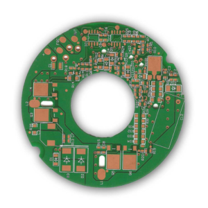
RF circuit PCB design
General layout principle: components should be arranged in the same direction as much as possible, and the phenomenon of poor welding can be reduced or even avoided by choosing the direction in which the PCB enters the tin melting system; according to experience, there must be at least 0.5mm spacing between components to meet the tin melting requirements of components. If the space of the PCB board allows, the spacing between components should be as wide as possible. For double-sided boards, one side should generally be designed with SMD and SMC components, and the other side should be discrete components.
Note in layout:
*First determine the position of the interface components with other PCB boards or systems on the PCB board, and pay attention to the coordination issues between the interface components (such as the direction of the components, etc.).
*Because the size of handheld products is very small and the components are arranged very compactly, larger components must be given priority, the corresponding positions must be determined, and the coordination issues between them must be considered.
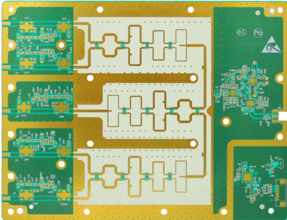
- Carefully analyze the circuit structure, process the circuit in blocks (such as high-frequency amplifier circuit, mixer circuit and demodulation circuit, etc.), separate strong electric signals from weak electric signals as much as possible, separate digital signal circuits from analog signal circuits, and arrange the circuits that complete the same function within a certain range as much as possible to reduce the signal loop area; the filter network of each part of the circuit must be connected nearby, which can not only reduce radiation, but also reduce the probability of interference, according to the anti-interference ability of the circuit.
- Group the unit circuits according to their different sensitivity to electromagnetic compatibility during use. When laying out the components that are susceptible to interference in the circuit, try to avoid interference sources (such as interference from the CPU on the data processing board, etc.).
4.Wiring
After the layout of the components is basically completed, wiring can be started. The basic principle of wiring is: when the assembly density permits, try to use low-density wiring design, and the signal routing should be as consistent as possible, which is conducive to impedance matching.
For RF circuits, unreasonable design of the direction, width, and line spacing of signal lines may cause cross interference between signal transmission lines; in addition, the system power supply itself also has noise interference, so comprehensive consideration must be given to reasonable wiring when designing the RF circuit PCB.
When wiring, all wiring should be kept away from the border of the PCB board (about 2mm) to avoid the risk of wire breakage or wire breakage during PCB board production.
The power line should be as wide as possible to reduce loop resistance. At the same time, the direction of the power line and ground line should be consistent with the direction of data transmission to improve anti-interference ability; the signal line should be as short as possible and the number of vias should be minimized; the connection between components should be as short as possible to reduce distributed parameters and mutual electromagnetic interference; incompatible signal lines should be kept away from each other, and parallel wiring should be avoided as much as possible, and the signal lines on the two sides of the positive direction should be perpendicular to each other; when wiring, the address where a corner is required should be 135°, and right angles should be avoided.
When wiring, the lines directly connected to the pads should not be too wide, and the routing should be kept away from unconnected components as much as possible to avoid short circuits; vias should not be drawn on components, and should be kept away from unconnected components as much as possible to avoid cold soldering, continuous soldering, short circuits, etc. in production.
In the PCB design of RF circuits, the correct routing of power lines and ground lines is particularly important, and reasonable design is the most important means to overcome electromagnetic interference. A considerable number of interference sources on PCBs are generated through power and ground lines, among which the noise interference caused by ground lines is the largest.
The main reason why ground lines are prone to electromagnetic interference is that there is impedance in the ground line. When current flows through the ground line, voltage will be generated on the ground line, thereby generating ground line loop current and forming ground line loop interference. When multiple circuits share a ground line, common impedance coupling will be formed, resulting in the so-called ground line noise. Therefore, when wiring the ground wire of the RF circuit PCB, the following should be done:
- First, the circuit is divided into blocks. The RF circuit can basically be divided into high-frequency amplification, mixing, demodulation, local oscillation and other parts. A common potential reference point, that is, the ground wire of each module circuit, should be provided for each circuit module, so that the signal can be transmitted between different circuit modules. Then, it is summarized at the place where the RF circuit PCB is connected to the ground wire, that is, the total ground wire. Since there is only one reference point, there is no common impedance coupling, and thus there is no mutual interference problem.
- The digital area and the analog area should be isolated by ground wire as much as possible, and the digital ground and the analog ground should be separated, and finally connected to the power ground.
- The ground wire inside each part of the circuit should also pay attention to the single-point grounding principle, minimize the signal loop area, and connect it to the address of the corresponding filter circuit nearby.
- If space permits, it is best to isolate each module with a ground wire to prevent signal coupling effects between each other.
5 Conclusion
The key to the design of RF circuit PCB lies in how to reduce radiation capability and how to improve anti-interference capability. Reasonable layout and wiring are the guarantee of designing RF circuit PCB. The method described in this article is beneficial to improving the reliability of RF circuit PCB design, solving the electromagnetic interference problem, and thus achieving the purpose of electromagnetic compatibility.