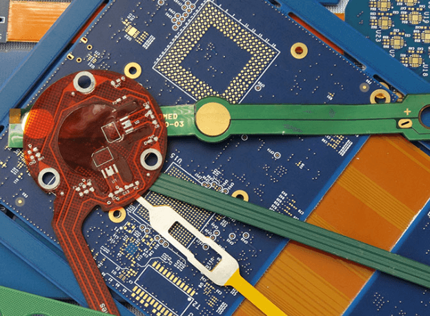
Rf flex pcb
Advantages Of Using RF Flex PCBs In Modern Electronics
RF flex PCBs, or radio frequency flexible printed circuit boards, have become increasingly integral in the realm of modern electronics. Their unique combination of flexibility, durability, and performance makes them an ideal choice for a wide range of applications.
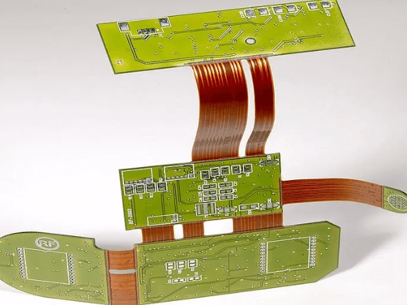
One of the primary advantages of RF flex PCBs is their ability to conform to complex shapes and fit into tight spaces, which is particularly beneficial in the design of compact and lightweight electronic devices. This adaptability not only enhances the aesthetic appeal of the final product but also allows for more innovative and ergonomic designs.
Moreover, RF flex PCBs offer superior signal integrity compared to their rigid counterparts.
The flexible nature of these PCBs reduces the risk of signal loss and interference, which is crucial in high-frequency applications. This is particularly important in the telecommunications industry, where maintaining signal clarity and strength is paramount. Additionally, the use of advanced materials in RF flex PCBs minimizes dielectric losses, further ensuring optimal performance in demanding environments.
Another significant advantage of RF flex PCBs is their enhanced reliability and durability.
The flexibility of these circuits allows them to withstand mechanical stress and vibrations better than rigid PCBs. This makes them ideal for use in automotive, aerospace, and industrial applications, where electronic components are often subjected to harsh conditions. Furthermore, the ability to bend and flex without breaking reduces the likelihood of circuit failure, thereby extending the lifespan of the device.
In addition to their mechanical benefits, RF flex PCBs also offer thermal advantages. The materials used in these PCBs typically have excellent thermal conductivity, which helps dissipate heat more effectively.
This is particularly beneficial in high-power applications, where managing heat is critical to maintaining performance and preventing damage.
The improved thermal management capabilities of RF flex PCBs contribute to the overall efficiency and reliability of electronic devices.
The manufacturing process of RF flex PCBs also presents several advantages. The ability to produce these circuits in a single, continuous piece reduces the need for connectors and interconnects, which can be potential points of failure. This not only simplifies the assembly process but also enhances the overall reliability of the device. Additionally, the use of flexible substrates allows for more efficient use of space, enabling the creation of smaller and lighter electronic products.
Furthermore, RF flex PCBs are highly customizable, allowing designers to tailor the circuits to meet specific requirements.
This level of customization is particularly valuable in the development of specialized electronic devices, where standard PCBs may not suffice. The ability to design and produce bespoke RF flex PCBs ensures that the final product meets the exact needs of the application, resulting in improved performance and functionality.
In conclusion, the advantages of using RF flex PCBs in modern electronics are manifold. Their flexibility, superior signal integrity, enhanced reliability, and thermal management capabilities make them an ideal choice for a wide range of applications. The manufacturing benefits and customization options further underscore their value in the development of innovative and high-performance electronic devices. As technology continues to advance, the role of RF flex PCBs in shaping the future of electronics is set to become even more significant.
Design Considerations For RF Flex PCBs
Designing RF flex PCBs requires meticulous attention to detail and a comprehensive understanding of both RF principles and flexible circuit technology. The unique characteristics of RF signals, combined with the inherent properties of flexible substrates, present a set of challenges that must be carefully navigated to ensure optimal performance.
One of the primary considerations in RF flex PCB design is the selection of materials.
The dielectric properties of the substrate play a crucial role in signal integrity, as they directly affect the propagation of RF signals. Materials with low dielectric constants and low loss tangents are preferred to minimize signal attenuation and phase distortion. Polyimide is a common choice due to its excellent thermal stability and mechanical flexibility, but other advanced materials like liquid crystal polymer (LCP) may also be considered for their superior electrical properties.
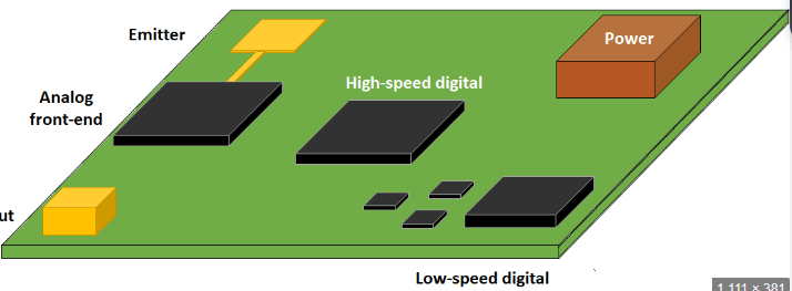
Another critical aspect is the layout of the transmission lines.
The geometry of these lines, including their width, spacing, and the thickness of the dielectric layer, must be precisely controlled to maintain the characteristic impedance. Microstrip and stripline configurations are commonly used, each with its own set of design rules. For instance, microstrip lines, which are placed on the surface of the substrate, require careful consideration of the ground plane placement to avoid unwanted radiation and crosstalk. Stripline configurations, on the other hand, are embedded within the substrate and offer better isolation but are more complex to manufacture.
Signal integrity is further influenced by the presence of bends and folds in the flexible PCB.
These physical deformations can introduce impedance discontinuities, leading to reflections and signal loss. To mitigate these effects, designers often employ gradual bends and maintain a consistent bend radius. Additionally, the use of ground planes and shielding can help to minimize electromagnetic interference (EMI) and ensure a stable signal path. The placement of components is another vital factor. Active and passive components must be strategically positioned to reduce parasitic effects and maintain signal integrity. For high-frequency applications, surface-mount technology (SMT) is generally preferred over through-hole components due to its lower parasitic inductance and capacitance. Furthermore, the use of via structures should be minimized, as they can introduce inductive and capacitive discontinuities that degrade signal performance.
Thermal management is also a significant concern in RF flex PCB design.
The flexible nature of the substrate can complicate heat dissipation, potentially leading to thermal hotspots and reliability issues. Effective thermal management strategies, such as the use of thermal vias, heat sinks, and conductive adhesives, are essential to ensure the longevity and performance of the PCB. In addition to these technical considerations, manufacturability and cost must also be taken into account. The complexity of RF flex PCB designs can drive up production costs and lead times. Therefore, it is crucial to work closely with manufacturers to optimize the design for cost-effective fabrication without compromising performance.
In conclusion, the design of RF flex PCBs is a multifaceted process that demands a deep understanding of both RF engineering and flexible circuit technology. By carefully selecting materials, optimizing transmission line layouts, managing signal integrity, and addressing thermal challenges, designers can create high-performance RF flex PCBs that meet the stringent requirements of modern electronic applications. Collaboration with experienced manufacturers further ensures that these designs are not only functional but also economically viable.
Common Applications Of RF Flex PCBs In Telecommunications
RF flex PCBs, or radio frequency flexible printed circuit boards, have become indispensable in the telecommunications industry due to their unique properties and versatile applications. These advanced circuit boards combine the benefits of flexibility with the capability to handle high-frequency signals, making them ideal for a range of telecommunications applications.
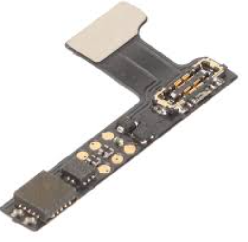
One of the primary uses of RF flex PCBs in telecommunications is in mobile devices.
As smartphones and tablets continue to evolve, the demand for compact, lightweight, and high-performance components has surged. RF flex PCBs meet these requirements by providing a flexible and durable solution that can be easily integrated into the compact spaces of modern mobile devices. Their ability to handle high-frequency signals ensures that these devices can maintain strong and reliable communication capabilities, even in challenging environments.
In addition to mobile devices, RF flex PCBs are also widely used in wireless communication systems.
These systems rely on high-frequency signals to transmit data over long distances, and the performance of the circuit boards used in these systems is critical to their overall efficiency. RF flex PCBs offer excellent signal integrity and low signal loss, making them ideal for use in base stations, antennas, and other critical components of wireless communication networks. Their flexibility allows for easy installation and maintenance, further enhancing their appeal in this application.
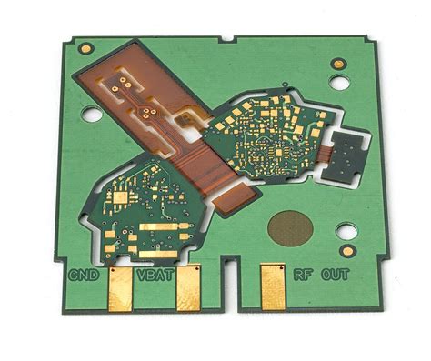
Another significant application of RF flex PCBs in telecommunications is in satellite communication systems.
Satellites require highly reliable and efficient components to ensure uninterrupted communication with ground stations and other satellites. RF flex PCBs are well-suited for this purpose due to their ability to withstand harsh environmental conditions, such as extreme temperatures and radiation. Their lightweight and flexible nature also make them ideal for use in the limited space available on satellites, where every gram of weight and millimeter of space is crucial.
Moreover, RF flex PCBs are increasingly being used in the development of Internet of Things (IoT) devices.
These devices rely on wireless communication to connect and share data, and the performance of their communication systems is critical to their overall functionality. RF flex PCBs provide the necessary high-frequency performance and flexibility to support the compact and often irregular shapes of IoT devices. This makes them an ideal choice for a wide range of applications, from smart home devices to industrial automation systems.
Furthermore, RF flex PCBs are also employed in the development of advanced radar systems.
These systems are used in various applications, including air traffic control, weather monitoring, and military operations. The high-frequency performance and reliability of RF flex PCBs make them suitable for use in these critical systems, where accurate and reliable signal transmission is essential. Their flexibility also allows for the design of more compact and lightweight radar systems, which can be easily deployed and maintained.
In conclusion, RF flex PCBs play a crucial role in the telecommunications industry, offering a range of benefits that make them ideal for various applications. From mobile devices and wireless communication systems to satellite communication and IoT devices, these advanced circuit boards provide the necessary performance, reliability, and flexibility to support the ever-evolving demands of modern telecommunications. As technology continues to advance, the importance of RF flex PCBs in telecommunications is only expected to grow, further solidifying their position as a key component in this dynamic industry.
Manufacturing Challenges And Solutions For RF Flex PCBs
Manufacturing RF flex PCBs presents a unique set of challenges that require specialized solutions to ensure optimal performance and reliability. These flexible printed circuit boards, designed to handle radio frequency signals, are increasingly in demand due to their ability to conform to complex geometries and their application in advanced electronics. However, the intricate nature of RF signals and the physical properties of flexible substrates introduce several manufacturing complexities.
One of the primary challenges in manufacturing RF flex PCBs is maintaining signal integrity.
RF signals are highly susceptible to interference and loss, which can be exacerbated by the flexible nature of the substrate. To address this, manufacturers must carefully select materials with low dielectric constants and minimal signal loss. Polyimide is a common choice due to its excellent electrical properties and flexibility. Additionally, the use of advanced simulation tools during the design phase can help predict and mitigate potential signal integrity issues.
Another significant challenge is the precise control of impedance.
Impedance matching is crucial for RF circuits to ensure maximum power transfer and minimal signal reflection. Variations in the thickness of the substrate, the width of the conductive traces, and the dielectric constant can all affect impedance. To achieve the required precision, manufacturers often employ controlled impedance techniques, which involve tightly regulated manufacturing processes and rigorous testing. This may include the use of laser direct structuring (LDS) to create highly accurate trace geometries.
Thermal management is also a critical concern in RF flex PCB manufacturing.
The flexible substrates used in these PCBs typically have lower thermal conductivity compared to rigid boards, making it challenging to dissipate heat generated by high-frequency components. Effective thermal management solutions include the incorporation of thermal vias, which help transfer heat away from critical areas, and the use of heat spreaders or thermal interface materials. Additionally, careful layout design can help distribute heat more evenly across the board.
The mechanical properties of flexible substrates introduce further manufacturing challenges.
Flex PCBs must withstand repeated bending and flexing without compromising their electrical performance or structural integrity. This requires the use of robust materials and advanced manufacturing techniques. For instance, the application of protective coatings can enhance the durability of the flex PCB, while the use of strain relief features can prevent damage to critical areas during flexing.
Moreover, the miniaturization trend in electronics adds another layer of complexity to RF flex PCB manufacturing.
As devices become smaller, the demand for compact and densely packed PCBs increases. This necessitates the use of fine-pitch components and high-density interconnects (HDI), which require advanced fabrication techniques such as microvia drilling and sequential lamination. Ensuring the reliability of these densely packed boards involves stringent quality control measures and thorough testing.
In conclusion, the manufacturing of RF flex PCBs involves addressing a range of challenges related to signal integrity, impedance control, thermal management, mechanical durability, and miniaturization. By leveraging advanced materials, precise manufacturing techniques, and rigorous testing protocols, manufacturers can overcome these challenges and produce high-performance RF flex PCBs. As the demand for flexible and high-frequency electronic solutions continues to grow, ongoing innovation and refinement in manufacturing processes will be essential to meet the evolving needs of the industry.