Rf pcb
Design Considerations for RF PCB Layout
Designing a radio frequency (RF) printed circuit board (PCB) requires meticulous attention to detail and a comprehensive understanding of electromagnetic principles. The complexity of RF signals, which operate at high frequencies, necessitates a distinct approach compared to standard PCB designs. To ensure optimal performance, several critical design considerations must be taken into account.
Firstly, the choice of materials is paramount. RF PCBs often utilize specialized substrates such as Rogers or Teflon, which offer superior dielectric properties compared to traditional FR-4 materials.
These substrates minimize signal loss and ensure consistent impedance, which is crucial for maintaining signal integrity at high frequencies. Additionally, the thickness of the substrate and the copper layers must be carefully selected to match the specific requirements of the RF application.
Transitioning to the layout, impedance control is a fundamental aspect of RF PCB design.
Impedance mismatches can lead to signal reflections, which degrade performance. To mitigate this, designers must ensure that transmission lines are precisely calculated and implemented. Microstrip and stripline configurations are commonly used, each offering distinct advantages depending on the application. Microstrip lines, for instance, are easier to implement but are more susceptible to external interference, whereas stripline configurations provide better isolation but are more complex to design.
Moreover, the placement of components plays a critical role in RF PCB design.
Components should be strategically positioned to minimize the length of signal paths, thereby reducing potential losses and interference. It is also essential to separate RF components from digital components to prevent cross-talk and other forms of electromagnetic interference. Ground planes are often employed to provide a return path for signals and to shield sensitive components from noise.
In addition to component placement, the routing of traces requires careful consideration.
RF traces should be as short and direct as possible to minimize inductance and resistance. Right-angle bends should be avoided, as they can cause impedance discontinuities. Instead, gradual curves or mitered bends are recommended to maintain signal integrity. Furthermore, the use of vias should be minimized, as they introduce additional inductance and can disrupt the signal path.
Thermal management is another critical consideration in RF PCB design.
High-frequency components can generate significant heat, which, if not properly managed, can affect performance and reliability. Designers must incorporate adequate thermal vias and heat sinks to dissipate heat effectively. Additionally, the choice of materials with good thermal conductivity can aid in managing heat dissipation.
Finally, electromagnetic compatibility (EMC) is a crucial aspect of RF PCB design.
Ensuring that the PCB does not emit or is not susceptible to electromagnetic interference is essential for compliance with regulatory standards and for the reliable operation of the device. Techniques such as shielding, filtering, and careful grounding can help achieve EMC compliance.
In conclusion, designing an RF PCB involves a complex interplay of material selection, impedance control, component placement, trace routing, thermal management, and EMC considerations. Each of these elements must be meticulously addressed to ensure the successful implementation of RF circuits. By adhering to these design principles, engineers can create RF PCBs that deliver high performance and reliability in a wide range of applications.
Material Selection for High-Frequency RF PCBs
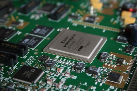
In the realm of high-frequency radio frequency (RF) printed circuit boards (PCBs), material selection plays a pivotal role in determining the performance and reliability of the final product. As RF PCBs are integral to a wide array of applications, from telecommunications to aerospace, understanding the nuances of material properties is essential for engineers and designers. The choice of substrate material can significantly influence the electrical performance, thermal management, and mechanical stability of the PCB, making it a critical consideration in the design process.
To begin with, dielectric constant (Dk) is a fundamental property that must be considered when selecting materials for high-frequency RF PCBs.
The dielectric constant affects the speed at which signals propagate through the material, and thus, materials with a stable and low Dk are often preferred for high-frequency applications. This stability ensures minimal signal distortion and loss, which is crucial for maintaining signal integrity. Materials such as PTFE (polytetrafluoroethylene) composites and ceramic-filled laminates are commonly used due to their low dielectric constants and excellent high-frequency performance.
In addition to dielectric constant, the dissipation factor (Df) is another critical parameter.
The dissipation factor measures the dielectric losses within the material, which can lead to signal attenuation and reduced efficiency. For high-frequency applications, materials with a low dissipation factor are desirable as they minimize energy loss and heat generation. This is particularly important in RF applications where maintaining signal strength and clarity is paramount. Advanced materials like Rogers and Taconic laminates are often selected for their low dissipation factors, which contribute to superior performance in demanding RF environments.
Thermal management is another crucial aspect of material selection for RF PCBs.
High-frequency applications often generate significant heat, which can affect the performance and longevity of the PCB. Therefore, materials with good thermal conductivity are essential to dissipate heat effectively and prevent overheating. Copper-clad laminates with enhanced thermal properties are frequently employed to address these challenges, ensuring that the PCB can operate reliably under high thermal loads.
Moreover, the mechanical properties of the substrate material should not be overlooked.
RF PCBs are often subjected to various environmental stresses, including vibration, mechanical shock, and temperature fluctuations. Consequently, materials with robust mechanical strength and dimensional stability are necessary to withstand these conditions without compromising performance. Materials like FR-4, although commonly used in standard PCBs, may not always meet the stringent requirements of high-frequency applications. Instead, specialized materials that offer a balance of mechanical resilience and electrical performance are preferred.
Furthermore, the cost and availability of materials are practical considerations that can influence material selection.
While high-performance materials may offer superior electrical and thermal properties, they can also be more expensive and less readily available. Therefore, designers must weigh the benefits of advanced materials against budget constraints and supply chain considerations. In some cases, a compromise between performance and cost may be necessary to achieve the desired balance.
In conclusion, selecting the appropriate material for high-frequency RF PCBs is a multifaceted decision that requires careful consideration of various electrical, thermal, and mechanical properties. By understanding the interplay between these factors, engineers can make informed choices that enhance the performance and reliability of RF PCBs in their specific applications. As technology continues to advance, ongoing research and development in material science will undoubtedly lead to new innovations and opportunities in the field of RF PCB design.
Techniques for Minimizing Signal Loss in RF PCBs
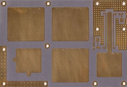
In the realm of radio frequency (RF) printed circuit boards (PCBs), minimizing signal loss is a critical concern for engineers and designers. As RF PCBs are integral to a wide array of applications, from telecommunications to aerospace, ensuring optimal performance is paramount. Signal loss, often referred to as insertion loss, can significantly degrade the performance of RF circuits, leading to inefficiencies and potential failures. Therefore, understanding and implementing techniques to minimize this loss is essential.
One of the primary techniques for minimizing signal loss in RF PCBs is the careful selection of materials.
The dielectric material used in the PCB can have a profound impact on signal integrity. Materials with low dielectric constant (Dk) and low dissipation factor (Df) are preferred, as they reduce the amount of energy lost as heat. For instance, materials such as PTFE (polytetrafluoroethylene) and certain ceramic-filled laminates are often chosen for their superior electrical properties. These materials help maintain signal strength by minimizing the attenuation that occurs as the signal propagates through the PCB.
In addition to material selection, the design of the PCB itself plays a crucial role in minimizing signal loss.
The layout of the traces, which carry the RF signals, must be meticulously planned. To reduce signal loss, it is advisable to keep trace lengths as short as possible, as longer traces can lead to increased resistance and, consequently, greater signal attenuation. Moreover, maintaining consistent trace widths and avoiding sharp bends can help preserve signal integrity. Sharp bends can cause reflections and impedance mismatches, which contribute to signal loss. Instead, using gradual curves and maintaining a uniform trace width can mitigate these issues.
Furthermore, impedance matching is a vital technique in minimizing signal loss.
Impedance mismatches between different components or sections of the PCB can lead to reflections, which in turn cause signal loss. By ensuring that the impedance of the traces matches that of the connected components, reflections can be minimized, thereby preserving signal strength. This can be achieved through careful calculation and design, often involving the use of simulation software to model and adjust the impedance characteristics of the PCB.
Another effective strategy is the use of ground planes and shielding.
Ground planes can help reduce electromagnetic interference (EMI) and crosstalk between traces, both of which can contribute to signal loss. By providing a return path for the RF signals, ground planes help maintain signal integrity. Additionally, shielding can be employed to protect sensitive components from external sources of interference. This is particularly important in environments with high levels of EMI, where unshielded components may experience significant signal degradation.
Finally, attention to detail in the manufacturing process is crucial.
Ensuring that the PCB is fabricated to high standards, with precise control over parameters such as trace width and spacing, can prevent unintentional variations that might lead to signal loss. Regular testing and quality control measures can help identify and rectify potential issues before they impact the performance of the final product.
In conclusion, minimizing signal loss in RF PCBs requires a multifaceted approach, encompassing material selection, design considerations, impedance matching, and manufacturing precision. By employing these techniques, engineers can enhance the performance and reliability of RF circuits, ensuring that they meet the demanding requirements of modern applications.

Challenges in Manufacturing RF PCBs
The manufacturing of Radio Frequency (RF) Printed Circuit Boards (PCBs) presents a unique set of challenges that distinguish it from the production of standard PCBs. As the demand for high-frequency applications continues to grow, driven by advancements in telecommunications, aerospace, and consumer electronics, the need for precise and reliable RF PCBs becomes increasingly critical. Understanding the complexities involved in their production is essential for manufacturers aiming to meet the stringent requirements of modern RF applications.
One of the primary challenges in manufacturing RF PCBs is the selection of suitable materials.
Unlike conventional PCBs, RF PCBs require materials with specific dielectric properties to ensure minimal signal loss and optimal performance at high frequencies. Materials such as PTFE (Polytetrafluoroethylene) and ceramic-filled laminates are often preferred due to their low dielectric constant and loss tangent. However, these materials can be difficult to handle and process, requiring specialized equipment and expertise. The choice of material not only affects the electrical performance but also impacts the thermal management and mechanical stability of the PCB, necessitating a careful balance between these factors.
Moreover, the design of RF PCBs demands meticulous attention to detail.
The layout must be optimized to minimize parasitic inductance and capacitance, which can degrade signal integrity. This involves precise control over trace widths, spacing, and the use of ground planes to provide effective shielding and reduce electromagnetic interference (EMI). The complexity of RF designs often requires advanced simulation tools to predict the behavior of the circuit under various conditions, adding another layer of complexity to the design process.
Transitioning from design to fabrication, the manufacturing process itself poses significant challenges.
The precision required in etching fine traces and maintaining tight tolerances is paramount to ensure the functionality of RF circuits. Any deviation can lead to impedance mismatches, resulting in signal reflection and loss. Additionally, the multilayer nature of many RF PCBs necessitates accurate layer alignment and registration, which can be difficult to achieve consistently. The use of advanced manufacturing techniques, such as laser drilling and controlled depth routing, is often necessary to meet these stringent requirements.
Furthermore, the assembly of RF PCBs introduces additional hurdles.
The components used in RF applications, such as surface-mount devices (SMDs) and connectors, must be placed with high precision to avoid performance degradation. The soldering process must be carefully controlled to prevent thermal damage to sensitive components and ensure reliable connections. The use of lead-free solder, mandated by environmental regulations, can complicate this process due to its higher melting point and different wetting characteristics compared to traditional leaded solder.
Finally, testing and quality assurance are critical stages in the production of RF PCBs.
Given the high frequencies involved, traditional testing methods may not suffice, necessitating the use of specialized equipment such as network analyzers and spectrum analyzers to verify performance. Ensuring that each PCB meets the required specifications is essential to avoid costly failures in the field.
In conclusion, the manufacturing of RF PCBs is a complex and demanding process that requires a deep understanding of materials, design principles, and fabrication techniques. As technology continues to advance, the challenges associated with producing these critical components will likely evolve, necessitating ongoing innovation and adaptation within the industry.


