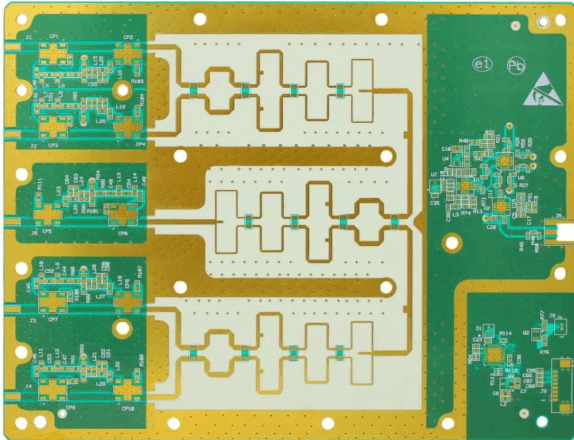
Rf pcb assembly
Key Considerations In RF PCB Assembly
RF PCB assembly, or Radio Frequency Printed Circuit Board assembly, is a specialized area within the broader field of PCB manufacturing that demands meticulous attention to detail and a deep understanding of high-frequency signal behavior.
As RF circuits operate at frequencies ranging from a few megahertz to several gigahertz, the assembly process must address unique challenges to ensure optimal performance and reliability. Key considerations in RF PCB assembly encompass material selection, signal integrity, thermal management, and component placement, each playing a crucial role in the overall functionality of the RF system.
To begin with, material selection is paramount in RF PCB assembly.
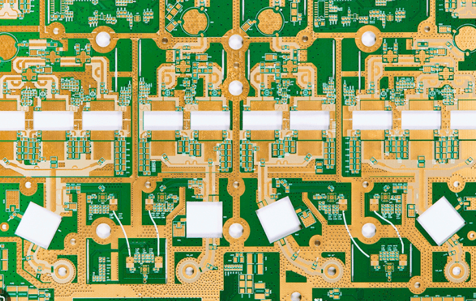
The dielectric material used in the PCB substrate significantly influences signal propagation and loss characteristics. High-frequency signals are particularly susceptible to dielectric losses, which can degrade signal integrity. Therefore, materials with low dielectric constant (Dk) and low dissipation factor (Df) are preferred. Common choices include PTFE (Polytetrafluoroethylene) and ceramic-filled laminates, which offer excellent electrical properties and stability over a wide frequency range. Additionally, the copper foil used in RF PCBs should have a smooth surface finish to minimize signal attenuation and ensure consistent impedance.
Signal integrity is another critical aspect that must be meticulously managed during RF PCB assembly.
High-frequency signals are prone to reflection, crosstalk, and electromagnetic interference (EMI), which can severely impact the performance of the RF circuit. To mitigate these issues, careful impedance control is essential. This involves designing transmission lines with precise dimensions and spacing to maintain consistent impedance throughout the signal path. Techniques such as microstrip and stripline configurations are commonly employed to achieve this. Furthermore, the use of ground planes and proper grounding techniques helps to reduce EMI and improve signal integrity.
Thermal management is also a vital consideration in RF PCB assembly.
High-frequency components, such as power amplifiers and oscillators, can generate significant amounts of heat during operation. Effective thermal management ensures that these components operate within their specified temperature ranges, thereby enhancing reliability and longevity. This can be achieved through the use of thermal vias, heat sinks, and thermal interface materials that facilitate efficient heat dissipation. Additionally, the layout of the PCB should be designed to minimize thermal resistance and ensure even heat distribution.
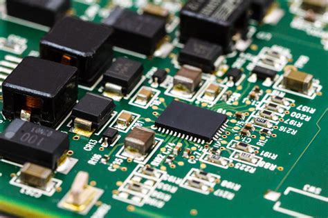
Component placement and routing are equally important in RF PCB assembly.
The placement of components must be carefully planned to minimize signal path lengths and avoid unnecessary bends or turns, which can introduce signal loss and distortion. Critical components, such as RF connectors and antennas, should be placed in locations that optimize signal transmission and reception. Moreover, the routing of high-frequency signals should be done with minimal layer transitions to reduce signal degradation. The use of controlled impedance traces and differential pairs can further enhance signal integrity.
In conclusion, RF PCB assembly is a complex and demanding process that requires a thorough understanding of high-frequency signal behavior and meticulous attention to detail. Key considerations, including material selection, signal integrity, thermal management, and component placement, must be carefully addressed to ensure the optimal performance and reliability of RF circuits. By adhering to these principles, manufacturers can produce RF PCBs that meet the stringent requirements of modern communication systems and other high-frequency applications.
Common Challenges In RF PCB Design And Assembly
Designing and assembling RF (Radio Frequency) PCBs (Printed Circuit Boards) present a unique set of challenges that require specialized knowledge and meticulous attention to detail.
One of the primary difficulties in RF PCB design is managing signal integrity.
High-frequency signals are particularly susceptible to interference and signal loss, which can significantly degrade performance. To mitigate these issues, designers must carefully consider the layout of the PCB, including the placement of components and the routing of traces.
Ensuring that traces are as short and direct as possible can help minimize signal degradation. Additionally, the use of ground planes and proper shielding techniques can further enhance signal integrity by reducing electromagnetic interference (EMI).
Another significant challenge in RF PCB design is impedance matching.
Impedance mismatches can lead to signal reflections, which can cause data errors and reduce the overall efficiency of the system. To address this, designers must calculate the characteristic impedance of the transmission lines and match it to the impedance of the components and connectors. This often involves the use of specialized software tools and precise manufacturing processes to ensure that the PCB meets the required specifications.
Thermal management is also a critical consideration in RF PCB assembly.
High-frequency components can generate significant amounts of heat, which can affect the performance and reliability of the PCB. Effective thermal management strategies, such as the use of heat sinks, thermal vias, and proper airflow design, are essential to dissipate heat and maintain optimal operating temperatures. Failure to adequately manage heat can result in component failure and reduced lifespan of the PCB.
Material selection is another crucial aspect of RF PCB design and assembly.
The choice of substrate material can have a significant impact on the performance of the PCB. Materials with low dielectric constants and low loss tangents are typically preferred for high-frequency applications, as they help minimize signal loss and distortion. However, these materials can be more expensive and challenging to work with, requiring specialized manufacturing techniques and equipment.
Moreover, the miniaturization of components and the increasing complexity of modern RF PCBs add another layer of difficulty to the design and assembly process.
As devices become smaller and more integrated, the density of components on the PCB increases, making it more challenging to maintain signal integrity and manage thermal issues. Advanced manufacturing techniques, such as surface-mount technology (SMT) and microvia technology, are often required to achieve the necessary level of precision and reliability.
Testing and validation are also critical steps in the RF PCB assembly process.
Ensuring that the PCB meets all performance specifications and operates correctly under various conditions is essential. This often involves extensive testing, including signal integrity analysis, thermal testing, and EMI testing. Any issues identified during testing must be addressed through design modifications or adjustments to the assembly process.
In conclusion, RF PCB design and assembly involve a complex interplay of factors that must be carefully managed to achieve optimal performance. From signal integrity and impedance matching to thermal management and material selection, each aspect presents its own set of challenges. By employing advanced design techniques, precise manufacturing processes, and thorough testing, it is possible to overcome these challenges and produce high-quality RF PCBs that meet the demanding requirements of modern applications.
Best Practices For RF PCB Component Placement
In the realm of RF PCB assembly, the meticulous placement of components is paramount to ensuring optimal performance and reliability. The intricate nature of RF circuits necessitates a strategic approach to component placement, as even minor deviations can lead to significant signal degradation or interference. To achieve the best results, several best practices should be adhered to during the design and assembly process.
Firstly, it is essential to consider the signal path and its integrity.
RF signals are highly susceptible to loss and interference, making it crucial to minimize the length of signal traces. By placing components in close proximity to each other, designers can reduce the potential for signal degradation. Additionally, maintaining a consistent impedance along the signal path is vital. This can be achieved by carefully controlling the trace width and spacing, as well as by using appropriate materials for the PCB substrate.
Another critical aspect of RF PCB component placement is the management of electromagnetic interference (EMI).
EMI can severely impact the performance of RF circuits, leading to noise and signal distortion. To mitigate EMI, components should be placed in a manner that minimizes coupling between high-frequency and low-frequency signals. Shielding techniques, such as the use of ground planes and metal enclosures, can also be employed to protect sensitive components from external interference.
Thermal management is another key consideration in RF PCB assembly.
High-frequency components often generate significant amounts of heat, which can affect their performance and longevity. To address this, components should be placed in a way that facilitates efficient heat dissipation. This may involve the use of thermal vias, heat sinks, or other cooling mechanisms. Additionally, ensuring adequate spacing between components can help prevent thermal coupling and reduce the risk of overheating.
Power integrity is equally important in RF PCB design.
Fluctuations in power supply can lead to instability and noise in RF circuits. To maintain a stable power supply, decoupling capacitors should be placed as close as possible to the power pins of active components. This helps to filter out noise and provide a steady voltage. Furthermore, the use of multiple ground planes can enhance power distribution and reduce the potential for ground loops.
The layout of passive components, such as resistors, capacitors, and inductors, also plays a crucial role in RF PCB performance.
These components should be placed in a manner that minimizes parasitic effects, such as inductance and capacitance, which can alter the behavior of the circuit. For instance, placing capacitors close to the signal path can help to filter out unwanted frequencies, while inductors should be oriented to minimize mutual coupling.
In addition to these technical considerations, it is important to follow industry standards and guidelines for RF PCB assembly.
Standards such as IPC-2221 and IPC-2223 provide valuable insights into best practices for component placement, trace routing, and other aspects of PCB design. Adhering to these standards can help ensure that the final product meets the required performance and reliability criteria.
In conclusion, the placement of components in RF PCB assembly is a complex and critical task that requires careful planning and attention to detail. By considering factors such as signal integrity, EMI management, thermal management, power integrity, and the layout of passive components, designers can optimize the performance of their RF circuits. Following industry standards and guidelines further enhances the reliability and effectiveness of the final product. Through these best practices, the challenges associated with RF PCB assembly can be effectively addressed, leading to superior performance and longevity of RF devices.
Advanced Techniques For RF PCB Signal Integrity
Ensuring signal integrity in RF PCB assembly is a critical aspect of modern electronics design, particularly as devices become more complex and operate at higher frequencies. Advanced techniques are essential to maintain the fidelity of RF signals, minimize interference, and ensure reliable performance.
One of the primary considerations in RF PCB design is the careful management of impedance.
Impedance mismatches can lead to signal reflections, which degrade signal quality and can cause data errors.
To address this, designers often employ controlled impedance traces, which involve precise control over the width and spacing of PCB traces to maintain a consistent impedance value. This technique is particularly important in high-frequency applications where even minor variations can have significant impacts.
Another crucial technique is the use of proper grounding practices.
A solid ground plane is essential for providing a return path for RF signals and minimizing electromagnetic interference (EMI). By ensuring a continuous ground plane, designers can reduce the potential for signal degradation and improve overall signal integrity. Additionally, the use of via stitching, which involves placing multiple vias around the perimeter of the ground plane, can further enhance grounding and reduce EMI.
Shielding is also a vital technique in RF PCB assembly.
By enclosing sensitive components and traces within a conductive shield, designers can protect them from external electromagnetic fields and prevent the emission of RF signals that could interfere with other components. This is particularly important in densely packed PCBs where components are in close proximity and the potential for interference is high. Effective shielding requires careful consideration of the materials used and the design of the shield to ensure it does not introduce additional impedance or signal loss.
The layout of the PCB itself plays a significant role in maintaining signal integrity.
Proper component placement and trace routing are essential to minimize signal path lengths and avoid unnecessary bends or loops, which can introduce inductance and capacitance that degrade signal quality. Designers often use simulation tools to model the PCB layout and identify potential issues before fabrication, allowing for adjustments to be made early in the design process.
In addition to these techniques, the choice of materials is critical in RF PCB assembly.
High-frequency signals are particularly sensitive to the dielectric properties of the PCB substrate. Materials with low dielectric constant and low loss tangent are preferred, as they minimize signal attenuation and phase distortion. Common materials used in RF PCBs include PTFE (Teflon) and ceramic-filled laminates, which offer excellent electrical performance but can be more challenging to work with compared to standard FR4 substrates.
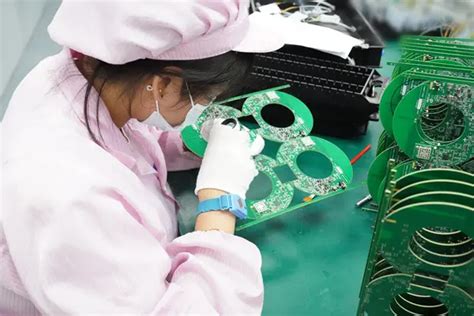
Finally, the assembly process itself must be carefully controlled to ensure signal integrity.
This includes precise placement of components, accurate soldering, and thorough inspection to detect any defects that could impact performance. Advanced assembly techniques such as automated optical inspection (AOI) and X-ray inspection are often employed to ensure the highest quality standards are met.
In conclusion, maintaining signal integrity in RF PCB assembly requires a comprehensive approach that encompasses impedance control, grounding, shielding, layout optimization, material selection, and meticulous assembly processes. By employing these advanced techniques, designers can ensure that their RF PCBs deliver reliable performance in even the most demanding applications.