Rf pcb manufacturing
Design Considerations for RF PCB Manufacturing
Designing printed circuit boards (PCBs) for radio frequency (RF) applications involves a unique set of challenges and considerations that differ significantly from those encountered in low-frequency or digital circuits.
The primary objective in RF PCB manufacturing is to ensure signal integrity and minimize losses, which requires meticulous attention to various design parameters. To achieve optimal performance, designers must consider factors such as material selection, trace layout, impedance control, and thermal management.
One of the first considerations in RF PCB design is the choice of substrate material.
Unlike standard PCBs, which often use FR-4 material, RF PCBs typically require substrates with lower dielectric constants and lower loss tangents. Materials such as Rogers, Taconic, or PTFE-based laminates are commonly used due to their superior high-frequency performance. These materials help to reduce signal attenuation and maintain signal integrity over longer distances. Additionally, the thermal properties of the substrate must be considered, as RF components can generate significant heat during operation.
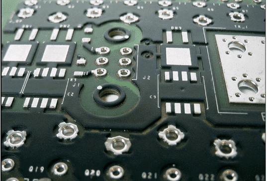
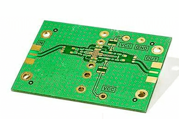
Trace layout is another critical aspect of RF PCB design.
The geometry and placement of traces can significantly impact signal performance. To minimize signal loss and crosstalk, designers often use microstrip or stripline configurations. Microstrip lines are traces on the outer layer of the PCB with a ground plane beneath them, while stripline traces are sandwiched between two ground planes within the PCB. Both configurations help to control impedance and reduce electromagnetic interference (EMI). Furthermore, maintaining consistent trace width and spacing is essential to ensure uniform impedance, which is crucial for signal integrity.
Impedance control is paramount in RF PCB manufacturing.
Impedance mismatches can lead to signal reflections, which degrade performance and cause signal loss. To achieve precise impedance control, designers must carefully calculate the trace width, spacing, and the dielectric properties of the substrate. Tools such as impedance calculators and simulation software are often employed to model and verify the impedance of the traces. Additionally, controlled impedance testing during the manufacturing process ensures that the PCB meets the required specifications.
Thermal management is another important consideration in RF PCB design.
High-frequency components can generate substantial heat, which can affect performance and reliability. Effective thermal management strategies include the use of thermal vias, heat sinks, and proper component placement to dissipate heat efficiently. Thermal vias are plated through-holes that connect the top and bottom layers of the PCB, allowing heat to transfer away from critical components. Heat sinks and thermal pads can also be used to enhance heat dissipation.
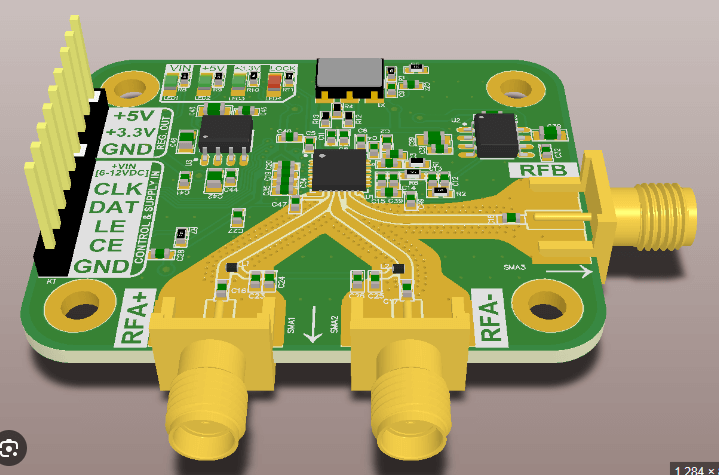
Moreover, the choice of components and their placement on the PCB can significantly impact RF performance.
Components such as capacitors, inductors, and resistors must be selected for their high-frequency characteristics. Surface-mount components are preferred over through-hole components due to their lower parasitic inductance and capacitance. Additionally, careful placement of components can minimize signal path lengths and reduce the potential for interference.
In conclusion, designing RF PCBs requires a comprehensive understanding of high-frequency principles and meticulous attention to detail. By carefully selecting substrate materials, optimizing trace layout, controlling impedance, managing thermal effects, and choosing appropriate components, designers can create RF PCBs that deliver superior performance and reliability. As RF technology continues to advance, the importance of these design considerations will only grow, making it essential for engineers to stay informed and adept in the latest RF PCB manufacturing techniques.
Material Selection in RF PCB Fabrication
In the realm of RF PCB manufacturing, the selection of materials plays a pivotal role in determining the performance, reliability, and overall success of the final product. The intricate nature of radio frequency (RF) circuits necessitates a meticulous approach to material selection, as the properties of the substrate and conductive materials directly influence signal integrity, impedance control, and thermal management. Consequently, understanding the key factors that guide material selection is essential for engineers and designers aiming to optimize their RF PCB designs.
To begin with, the dielectric constant (Dk) of the substrate material is a critical parameter in RF PCB fabrication.
The dielectric constant affects the propagation speed of electromagnetic waves through the substrate, thereby influencing the impedance and signal integrity of the circuit. Materials with a low and stable dielectric constant, such as PTFE (polytetrafluoroethylene) and certain ceramic-filled laminates, are often preferred for high-frequency applications. These materials minimize signal loss and ensure consistent performance across a wide frequency range.
Additionally, the dielectric loss tangent (Df) is another important consideration, as it quantifies the energy dissipation within the substrate. Low-loss materials are essential for maintaining signal strength and reducing attenuation in RF circuits.
Transitioning to the thermal properties of the substrate, thermal conductivity and coefficient of thermal expansion (CTE) are paramount.
RF circuits often generate significant heat, and efficient thermal management is crucial to prevent performance degradation and ensure longevity. High thermal conductivity materials, such as certain ceramic-filled laminates, facilitate effective heat dissipation, thereby maintaining optimal operating temperatures. Moreover, a low CTE is desirable to minimize mechanical stress and potential delamination during thermal cycling, which is particularly important in applications subjected to varying environmental conditions.
In addition to the substrate, the choice of conductive materials is equally significant.
Copper is the most commonly used conductor in RF PCB manufacturing due to its excellent electrical conductivity and relatively low cost. However, the surface finish of the copper traces can impact signal integrity, especially at high frequencies. Electroless nickel immersion gold (ENIG) and immersion silver are popular surface finishes that provide a smooth and stable interface, reducing signal loss and ensuring reliable performance. Furthermore, the thickness of the copper layer must be carefully controlled to achieve the desired impedance and minimize signal attenuation.
Another crucial aspect of material selection is the compatibility with the manufacturing process.
The chosen materials must be amenable to standard PCB fabrication techniques, including etching, drilling, and lamination. For instance, PTFE-based substrates require specialized processing due to their unique properties, such as high thermal stability and chemical resistance. Therefore, collaboration with experienced PCB manufacturers is essential to ensure that the selected materials can be effectively integrated into the production workflow.
Moreover, environmental and regulatory considerations cannot be overlooked in RF PCB manufacturing.
The materials used must comply with industry standards and regulations, such as RoHS (Restriction of Hazardous Substances) and REACH (Registration, Evaluation, Authorization, and Restriction of Chemicals). These regulations mandate the use of environmentally friendly and safe materials, thereby ensuring the sustainability and safety of the final product.
In conclusion, material selection in RF PCB fabrication is a multifaceted process that demands careful consideration of various electrical, thermal, mechanical, and regulatory factors. By selecting appropriate materials that align with the specific requirements of the application, engineers can enhance the performance, reliability, and longevity of RF circuits. As technology continues to advance, ongoing research and development in material science will undoubtedly yield new innovations, further optimizing the capabilities of RF PCB manufacturing.
Challenges in High-Frequency PCB Manufacturing
The manufacturing of radio frequency (RF) printed circuit boards (PCBs) presents a unique set of challenges that distinguish it from the production of standard PCBs. As the demand for high-frequency applications continues to grow, driven by advancements in telecommunications, aerospace, and defense industries, the need for precision and reliability in RF PCB manufacturing becomes increasingly critical.
One of the primary challenges in this domain is the selection of appropriate materials.
Unlike conventional PCBs, RF PCBs require substrates with low dielectric constants and low loss tangents to minimize signal attenuation and ensure signal integrity. Materials such as PTFE (polytetrafluoroethylene) and ceramic-filled laminates are often used, but they come with their own set of processing difficulties, including higher costs and more complex handling requirements.
In addition to material selection, the design and layout of RF PCBs pose significant hurdles.
High-frequency signals are highly susceptible to interference and signal loss, necessitating meticulous attention to trace width, spacing, and impedance control. The implementation of controlled impedance is crucial to maintaining signal integrity, which requires precise calculations and adherence to design specifications. Furthermore, the integration of components such as filters, amplifiers, and antennas must be carefully planned to avoid unwanted coupling and crosstalk. This level of precision often demands advanced simulation tools and iterative design processes, adding to the complexity and time required for development.
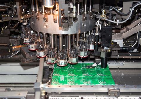
Another critical aspect of RF PCB manufacturing is the fabrication process itself.
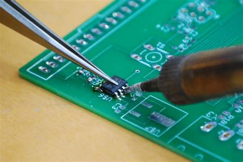
The etching of fine traces and the drilling of microvias require advanced equipment and techniques to achieve the necessary precision. Any deviation in the manufacturing process can lead to significant performance degradation, making quality control and testing paramount. Techniques such as automated optical inspection (AOI) and X-ray inspection are commonly employed to ensure the integrity of the PCB. Additionally, the assembly process must account for the thermal management of high-frequency components, as excessive heat can adversely affect performance and reliability. This often involves the use of specialized soldering techniques and thermal interface materials.
Moreover, the testing and validation of RF PCBs present their own set of challenges.
High-frequency testing requires specialized equipment and expertise to accurately measure parameters such as return loss, insertion loss, and phase stability. The testing environment must be carefully controlled to avoid external interference, and the interpretation of test results requires a deep understanding of RF principles. This level of scrutiny is essential to ensure that the final product meets the stringent performance requirements of high-frequency applications.
In conclusion, the manufacturing of RF PCBs is a complex and demanding process that requires careful consideration of materials, design, fabrication, and testing. Each stage presents its own set of challenges, necessitating a high level of expertise and precision. As the demand for high-frequency applications continues to rise, the industry must continue to innovate and refine its processes to meet the evolving needs of the market. The successful production of RF PCBs not only hinges on advanced technology and equipment but also on the skill and experience of the engineers and technicians involved. Through continuous improvement and adherence to best practices, the challenges of high-frequency PCB manufacturing can be effectively managed, ensuring the delivery of reliable and high-performance products.
Advanced Techniques in RF PCB Prototyping
In the realm of modern electronics, the demand for high-frequency applications has led to significant advancements in the manufacturing of Radio Frequency (RF) Printed Circuit Boards (PCBs). RF PCB prototyping, in particular, has evolved to incorporate advanced techniques that ensure optimal performance and reliability. These techniques are crucial for applications ranging from telecommunications to aerospace, where precision and efficiency are paramount.
One of the foremost considerations in RF PCB manufacturing is the selection of appropriate materials.
Unlike standard PCBs, RF PCBs require substrates with low dielectric constants and minimal loss tangents to maintain signal integrity at high frequencies. Materials such as Rogers, Taconic, and PTFE (Polytetrafluoroethylene) are commonly used due to their superior electrical properties. The choice of material directly impacts the performance of the RF circuit, making it a critical step in the prototyping process.
In addition to material selection, the design of the RF PCB layout plays a pivotal role in minimizing signal loss and interference.
Advanced techniques such as controlled impedance routing and differential pair routing are employed to ensure that the signal paths are optimized for high-frequency transmission. Controlled impedance routing involves maintaining a consistent impedance along the signal traces, which is essential for preventing signal reflections and ensuring signal integrity. Differential pair routing, on the other hand, involves routing two complementary signals together to reduce electromagnetic interference (EMI) and crosstalk.
Furthermore, the implementation of via structures in RF PCB prototyping requires meticulous attention.
Vias, which are used to connect different layers of the PCB, can introduce parasitic inductance and capacitance, adversely affecting the performance of high-frequency circuits. To mitigate these effects, techniques such as back-drilling and via-in-pad are employed. Back-drilling involves removing the unused portion of the via to reduce its inductance, while via-in-pad places the via directly under the component pad, minimizing the signal path length and associated parasitics.
Another advanced technique in RF PCB prototyping is the use of electromagnetic simulation tools.
These tools enable designers to model and analyze the electromagnetic behavior of the PCB layout before fabrication. By simulating the RF performance, designers can identify potential issues such as signal reflections, impedance mismatches, and EMI, allowing for adjustments to be made early in the design process. This not only enhances the performance of the final product but also reduces the time and cost associated with iterative prototyping.
Moreover, the precision of the manufacturing process itself is paramount in RF PCB prototyping.
Advanced fabrication techniques such as laser direct imaging (LDI) and precision etching are employed to achieve the fine geometries required for high-frequency circuits. LDI allows for the direct transfer of the PCB layout onto the substrate with high accuracy, while precision etching ensures that the copper traces are formed with minimal deviations. These techniques contribute to the overall performance and reliability of the RF PCB.
In conclusion, the advanced techniques employed in RF PCB prototyping are essential for meeting the stringent requirements of high-frequency applications. From material selection and layout design to via implementation and electromagnetic simulation, each step in the prototyping process is meticulously executed to ensure optimal performance. As technology continues to advance, the methods and tools used in RF PCB manufacturing will undoubtedly evolve, further enhancing the capabilities and applications of high-frequency electronic devices.