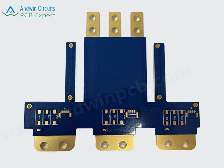
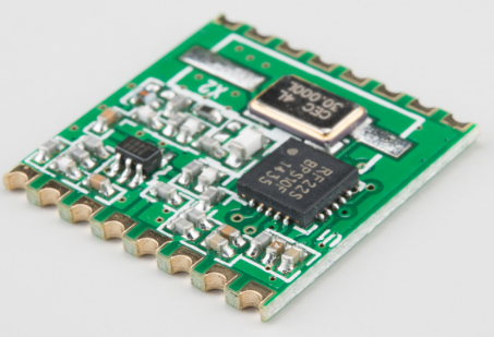
Rf pcb routing
Best Practices For RF PCB Routing
In the realm of electronics design, RF PCB routing stands as a critical component that demands meticulous attention to detail and adherence to best practices. The complexity of RF circuits, which operate at high frequencies, necessitates a nuanced approach to ensure signal integrity and optimal performance. As such, understanding the best practices for RF PCB routing is essential for engineers and designers aiming to create efficient and reliable RF systems.
To begin with, one of the fundamental principles in RF PCB routing is the minimization of signal path lengths.
Shorter paths reduce the potential for signal loss and minimize the risk of interference, which is particularly crucial at high frequencies. This can be achieved by strategically placing components in close proximity to each other, thereby reducing the distance that signals must travel. Additionally, maintaining a consistent trace width is vital, as variations can lead to impedance mismatches, which in turn can cause signal reflections and degrade performance.
Moreover, the use of ground planes is another best practice that cannot be overstated.
Ground planes serve as a reference point for signals and help in reducing electromagnetic interference (EMI). By providing a low-impedance path for return currents, ground planes enhance signal integrity and contribute to the overall stability of the circuit. It is advisable to ensure that the ground plane is continuous and unbroken, as any discontinuities can lead to increased inductance and potential signal degradation.
Transitioning to the topic of trace routing, it is important to consider the use of microstrip and stripline configurations.
Microstrip lines, which are traces on the outer layers of the PCB, are often used for their simplicity and ease of access. However, they are more susceptible to external interference. On the other hand, stripline configurations, which are sandwiched between two ground planes, offer better shielding and are preferred for high-frequency applications. The choice between these configurations should be guided by the specific requirements of the design and the operating environment.
Furthermore, impedance matching is a critical aspect of RF PCB routing.
Mismatched impedances can lead to signal reflections, which can severely impact the performance of the circuit. To achieve proper impedance matching, designers must carefully calculate the trace width and spacing, taking into account the dielectric properties of the PCB material. Tools such as impedance calculators and simulation software can be invaluable in this process, allowing for precise adjustments and optimization.
In addition to these considerations, the use of vias should be approached with caution.
While vias are necessary for connecting different layers of a PCB, they introduce inductance and capacitance, which can affect high-frequency signals. Minimizing the number of vias and ensuring they are placed strategically can help mitigate these effects. When vias are unavoidable, using blind or buried vias can reduce their impact on signal integrity.
Finally, it is essential to conduct thorough testing and validation of the RF PCB design.
Prototyping and iterative testing allow designers to identify and rectify potential issues before mass production. By employing network analyzers and other diagnostic tools, engineers can ensure that the PCB meets the desired specifications and performs reliably under various conditions.
In conclusion, RF PCB routing is a complex but manageable task when approached with a clear understanding of best practices. By focusing on minimizing signal path lengths, utilizing ground planes, selecting appropriate trace configurations, ensuring impedance matching, and carefully managing vias, designers can create robust RF circuits that deliver high performance and reliability.

Common Mistakes In RF PCB Design
In the realm of RF PCB design, precision and attention to detail are paramount. However, even seasoned engineers can fall prey to common mistakes that can compromise the performance and reliability of RF circuits. Understanding these pitfalls is crucial for anyone involved in the design and development of RF PCBs.
One of the most prevalent errors is the improper management of impedance.
RF signals are highly sensitive to impedance mismatches, which can lead to signal reflections and loss. To mitigate this, designers must ensure that transmission lines are carefully matched to the characteristic impedance of the system. This involves meticulous calculations and the use of appropriate materials and geometries to maintain consistent impedance throughout the circuit.
Another frequent mistake is inadequate grounding.
In RF PCB design, a solid and continuous ground plane is essential for minimizing electromagnetic interference and ensuring signal integrity. Interruptions in the ground plane, such as slots or gaps, can create unwanted inductance and capacitance, leading to performance degradation. Therefore, designers should strive to maintain an unbroken ground plane and use vias judiciously to connect different layers, thereby reducing the risk of ground loops and other related issues.
Moreover, the placement of components plays a critical role in RF PCB design.
Poor component placement can result in increased parasitic capacitance and inductance, which can adversely affect the circuit’s performance. To avoid this, components should be placed as close as possible to minimize trace lengths and reduce the potential for unwanted coupling. Additionally, sensitive components should be shielded from high-frequency noise sources, and care should be taken to separate analog and digital sections to prevent interference.
Transitioning to another common oversight, the routing of RF traces demands careful consideration.
Designers often make the mistake of routing RF traces in a manner that introduces sharp bends or corners. Such practices can cause impedance discontinuities and signal reflections, which degrade signal quality. Instead, RF traces should be routed with smooth curves and gentle bends to maintain consistent impedance and minimize signal loss. Furthermore, the use of microstrip or stripline configurations can help achieve better control over trace impedance.
In addition to routing, the selection of materials is a critical aspect that is sometimes overlooked.
The dielectric constant and loss tangent of the substrate material can significantly impact the performance of RF circuits. Choosing the wrong material can lead to increased signal attenuation and reduced efficiency. Therefore, it is essential to select materials that are specifically designed for RF applications, taking into account factors such as frequency range and environmental conditions.
Finally, inadequate testing and validation can lead to unforeseen issues in RF PCB design.
Designers may neglect thorough testing due to time constraints or budget limitations, but this can result in costly rework and delays. Comprehensive testing, including simulations and real-world measurements, is vital to ensure that the design meets all specifications and performs as intended under various conditions.
In conclusion, while RF PCB design presents unique challenges, being aware of common mistakes can significantly enhance the likelihood of success. By paying close attention to impedance management, grounding, component placement, trace routing, material selection, and testing, designers can create robust and reliable RF circuits that meet the demands of modern applications. Through careful planning and execution, the pitfalls of RF PCB design can be effectively navigated, leading to superior performance and functionality.
Advanced Techniques For RF Signal Integrity
In the realm of radio frequency (RF) design, maintaining signal integrity is paramount, particularly when it comes to printed circuit board (PCB) routing. As RF signals are highly susceptible to interference and loss, advanced techniques in RF PCB routing are essential to ensure optimal performance. Understanding these techniques requires a comprehensive grasp of the principles that govern RF behavior, as well as the practical considerations that influence design decisions.
To begin with, one of the fundamental aspects of RF PCB routing is impedance control.
Impedance mismatches can lead to signal reflections, which degrade signal integrity. Therefore, maintaining consistent impedance throughout the RF path is crucial. This can be achieved by carefully designing the trace width and spacing, as well as selecting appropriate materials for the PCB substrate. The use of microstrip or stripline configurations is common, as these structures allow for controlled impedance environments. Moreover, employing simulation tools to model and predict impedance characteristics can significantly enhance the accuracy of the design.
Transitioning to another critical consideration, the minimization of crosstalk is essential in RF PCB routing.
Crosstalk occurs when signals on adjacent traces interfere with each other, leading to unwanted noise and signal degradation. To mitigate this, designers often increase the spacing between RF traces and employ ground planes to provide isolation. Additionally, the use of guard traces, which are grounded traces placed between signal lines, can further reduce crosstalk by absorbing and redirecting interference.
Furthermore, the management of signal losses is a pivotal aspect of RF PCB routing.
Signal losses can occur due to dielectric losses, conductor losses, and radiation losses. To address these, selecting low-loss dielectric materials and optimizing trace geometry are effective strategies. For instance, using wider traces can reduce conductor losses, while minimizing the length of RF paths can decrease radiation losses. Additionally, incorporating vias with care is important, as they can introduce inductance and capacitance that affect signal integrity. Ensuring that vias are properly placed and minimized in number can help maintain signal quality.
In addition to these considerations, the integration of proper grounding techniques is vital for RF signal integrity.
A well-designed ground plane not only provides a return path for signals but also acts as a shield against electromagnetic interference (EMI). Ensuring that the ground plane is continuous and free of gaps is essential. Moreover, connecting the ground plane to the chassis ground at multiple points can further enhance EMI shielding.
As we delve deeper into advanced techniques, the use of differential signaling emerges as a powerful method for improving RF signal integrity.
Differential pairs, which consist of two complementary signals, are less susceptible to external noise and can effectively cancel out common-mode interference. This technique is particularly beneficial in environments with high levels of EMI.
Finally, it is important to consider the role of design for manufacturability (DFM) in RF PCB routing.
While advanced techniques can significantly enhance signal integrity, they must also be feasible for production. Collaborating with manufacturers early in the design process can ensure that the chosen routing strategies are compatible with manufacturing capabilities and cost constraints.
In conclusion, advanced techniques in RF PCB routing are essential for maintaining signal integrity in high-frequency applications. By focusing on impedance control, crosstalk minimization, loss management, grounding, differential signaling, and manufacturability, designers can create robust RF circuits that perform reliably in demanding environments. As technology continues to evolve, staying abreast of the latest advancements in RF PCB routing will remain a critical component of successful RF design.
Material Selection For RF PCB Applications
In the realm of radio frequency (RF) printed circuit board (PCB) design, material selection plays a pivotal role in determining the performance and reliability of the final product. As RF applications continue to expand across various industries, from telecommunications to aerospace, the demand for high-performance PCBs has never been greater. Consequently, understanding the nuances of material selection becomes essential for engineers and designers aiming to optimize their RF circuits.
To begin with, the dielectric constant (Dk) of the substrate material is a critical factor in RF PCB applications.
The dielectric constant affects the signal speed and impedance of the circuit, which in turn influences the overall performance of the RF system. Materials with a low and stable Dk are often preferred, as they allow for faster signal propagation and better impedance control. For instance, PTFE (polytetrafluoroethylene) and ceramic-filled laminates are popular choices due to their low dielectric constants and excellent thermal stability.
Moreover, the loss tangent, or dissipation factor, is another crucial parameter to consider.
This factor measures the inherent energy loss of the dielectric material as the RF signal passes through it. A lower loss tangent indicates that less signal energy is lost as heat, which is particularly important in high-frequency applications where signal integrity is paramount. Materials such as Rogers RO3000 series and Taconic RF-35 are renowned for their low loss tangents, making them suitable for high-frequency RF applications.
In addition to electrical properties, thermal management is a significant consideration in RF PCB material selection.
RF circuits often generate substantial heat, which can affect performance and reliability if not properly managed. Therefore, materials with high thermal conductivity are desirable, as they facilitate efficient heat dissipation. Copper-clad laminates with ceramic fillers are often employed for their superior thermal management capabilities, ensuring that the RF PCB can operate effectively under high-power conditions.
Furthermore, the mechanical properties of the substrate material should not be overlooked.
RF PCBs may be subjected to various environmental stresses, including vibration, shock, and temperature fluctuations. Therefore, materials with robust mechanical properties are essential to ensure the longevity and durability of the PCB. For example, materials like FR-4, while commonly used in general PCB applications, may not always meet the stringent requirements of RF applications due to their higher dielectric constant and loss tangent. Instead, materials specifically designed for RF applications, such as PTFE composites, offer better mechanical stability and performance.
Additionally, cost considerations often influence material selection for RF PCBs.
While high-performance materials can significantly enhance the performance of RF circuits, they also tend to be more expensive. Therefore, a balance must be struck between performance requirements and budget constraints. Engineers must carefully evaluate the trade-offs between cost and performance to select the most appropriate material for their specific application.
In conclusion, selecting the right material for RF PCB applications is a multifaceted process that requires careful consideration of various electrical, thermal, mechanical, and economic factors. By understanding the implications of each material property and how they interact with the specific requirements of the RF application, engineers can make informed decisions that optimize the performance and reliability of their RF circuits. As technology continues to advance, the importance of meticulous material selection in RF PCB design will only grow, underscoring its critical role in the development of cutting-edge RF technologies.