Rf pcb rules
Key Design Considerations for RF PCB Layout
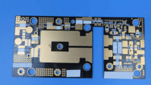
When designing a Radio Frequency (RF) Printed Circuit Board (PCB), several key considerations must be taken into account to ensure optimal performance and reliability. The complexity of RF signals, which operate at high frequencies, necessitates meticulous attention to detail in the layout process.
One of the primary considerations is impedance control.
Maintaining consistent impedance throughout the signal path is crucial to minimize signal reflections and losses. This can be achieved by carefully designing the trace widths and spacing, as well as selecting appropriate materials with consistent dielectric properties.
Another critical aspect is the management of signal integrity.
High-frequency signals are susceptible to various forms of interference, including crosstalk and electromagnetic interference (EMI). To mitigate these issues, designers should implement proper grounding techniques. A solid ground plane is essential, as it provides a low-impedance path for return currents and helps to shield sensitive components from external noise. Additionally, the use of via stitching can enhance the effectiveness of the ground plane by ensuring a continuous ground connection across different layers of the PCB.
Thermal management is also a significant consideration in RF PCB design.
High-frequency components often generate substantial amounts of heat, which can affect performance and reliability if not properly managed. Effective thermal management strategies include the use of thermal vias, heat sinks, and careful placement of heat-generating components to ensure adequate heat dissipation. Moreover, selecting materials with good thermal conductivity can help to distribute heat more evenly across the PCB.
Component placement is another vital factor in RF PCB layout.
The proximity of components can influence signal integrity and overall performance. Critical components, such as oscillators and amplifiers, should be placed as close to each other as possible to minimize signal path lengths and reduce potential interference. Additionally, sensitive components should be isolated from noisy elements to prevent unwanted coupling. The use of shielding can further protect sensitive areas from external noise sources.
The choice of PCB materials also plays a significant role in RF design.
Materials with low dielectric loss and stable dielectric constants are preferred, as they help to maintain signal integrity at high frequencies. Common materials used in RF PCB design include Rogers and Teflon-based substrates, which offer superior performance compared to traditional FR4 materials. However, these specialized materials can be more expensive, so a cost-benefit analysis is often necessary to determine the most suitable option for a given application.
Furthermore, the use of simulation tools can greatly enhance the design process.
Electromagnetic simulation software allows designers to model and analyze the behavior of RF signals within the PCB, identifying potential issues before physical prototyping. This can save time and resources by enabling designers to make informed decisions and optimize the layout for performance and manufacturability.
In conclusion, designing an RF PCB requires careful consideration of various factors, including impedance control, signal integrity, thermal management, component placement, material selection, and the use of simulation tools. By addressing these key considerations, designers can create RF PCBs that deliver reliable performance and meet the stringent demands of high-frequency applications. The complexity of RF design underscores the importance of a methodical and informed approach, ensuring that each aspect of the layout is meticulously planned and executed.
Essential RF PCB Material Selection Guidelines
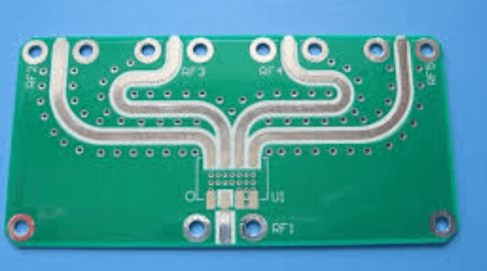
When designing a Radio Frequency (RF) Printed Circuit Board (PCB), the selection of materials is a critical factor that significantly influences the performance, reliability, and manufacturability of the final product. The choice of substrate material, in particular, plays a pivotal role in determining the electrical properties, thermal management, and mechanical stability of the RF PCB. Therefore, understanding the essential guidelines for RF PCB material selection is paramount for engineers and designers aiming to achieve optimal results.
To begin with, the dielectric constant (Dk) of the substrate material is a fundamental parameter that must be carefully considered.
The dielectric constant affects the signal propagation speed and impedance of the transmission lines. Materials with a low and stable dielectric constant are generally preferred for high-frequency applications, as they minimize signal loss and ensure consistent performance across a wide range of frequencies. For instance, materials such as PTFE (Polytetrafluoroethylene) and ceramic-filled laminates are commonly used in RF PCB designs due to their low Dk values and excellent high-frequency characteristics.
In addition to the dielectric constant, the dissipation factor (Df) is another crucial property that impacts the performance of RF PCBs.
The dissipation factor measures the dielectric losses within the substrate material, which can lead to signal attenuation and reduced efficiency. Low dissipation factor materials are essential for minimizing energy loss and maintaining signal integrity, especially in high-frequency applications. Consequently, materials with low Df values, such as Rogers RO4000 series and Taconic RF-35, are often selected for RF PCB designs.
Thermal management is another critical aspect that must be addressed when selecting RF PCB materials.
High-frequency circuits can generate significant amounts of heat, which, if not properly managed, can lead to performance degradation and potential failure of the PCB. Therefore, materials with good thermal conductivity and stability are essential to ensure efficient heat dissipation and maintain the reliability of the RF PCB. For example, materials like Rogers RT/duroid 6002 and Arlon AD450 exhibit excellent thermal properties, making them suitable choices for high-power RF applications.
Mechanical stability is also a key consideration in RF PCB material selection.
The substrate material must be able to withstand the mechanical stresses and environmental conditions encountered during the manufacturing process and throughout the operational life of the PCB. Factors such as coefficient of thermal expansion (CTE), moisture absorption, and dimensional stability must be evaluated to ensure the material can maintain its integrity and performance under varying conditions. Materials with low CTE and high dimensional stability, such as ceramic-filled PTFE composites, are often preferred for their robustness and reliability.
Furthermore, manufacturability is an important factor that cannot be overlooked.
The selected material must be compatible with standard PCB fabrication processes to ensure cost-effective and efficient production. Materials that are difficult to process or require specialized equipment can increase manufacturing complexity and costs. Therefore, it is essential to choose materials that offer a good balance between performance and ease of fabrication. For instance, materials like FR-4, although not ideal for very high-frequency applications, are widely used due to their excellent manufacturability and cost-effectiveness for lower frequency RF designs.
In conclusion, the selection of materials for RF PCBs is a multifaceted process that requires careful consideration of various electrical, thermal, mechanical, and manufacturability properties. By adhering to these essential guidelines, engineers and designers can ensure the development of high-performance, reliable, and cost-effective RF PCBs that meet the stringent demands of modern high-frequency applications.

Best Practices for RF PCB Signal Integrity
Ensuring signal integrity in RF PCB design is paramount for achieving optimal performance in high-frequency applications. The complexity of RF circuits necessitates meticulous attention to detail and adherence to best practices to mitigate issues such as signal loss, interference, and noise.
One of the fundamental principles in RF PCB design is the careful management of impedance.
Maintaining consistent impedance throughout the signal path is crucial, as impedance mismatches can lead to signal reflections, which degrade signal integrity. To achieve this, designers must precisely control the width and spacing of transmission lines, taking into account the dielectric properties of the PCB material.
In addition to impedance control, the layout of the PCB plays a significant role in maintaining signal integrity.
Minimizing the length of signal paths is essential to reduce the potential for signal degradation. Furthermore, the use of ground planes is a common practice to provide a return path for signals and to shield sensitive components from electromagnetic interference (EMI). Ground planes should be continuous and unbroken to ensure a low-impedance path for return currents, which helps in reducing noise and crosstalk between adjacent signal traces.
Another critical aspect of RF PCB design is the placement of components.
Strategic component placement can significantly impact the performance of the circuit. High-frequency components should be placed as close to each other as possible to minimize the length of interconnecting traces. Additionally, sensitive components should be isolated from noisy elements to prevent interference. This can be achieved by creating separate ground planes or using shielding techniques to protect sensitive areas of the PCB.
The choice of materials for the PCB is also a vital consideration.
High-frequency signals are more susceptible to losses due to the dielectric properties of the PCB substrate. Therefore, selecting a low-loss material with stable dielectric properties over the operating frequency range is essential. Materials such as Rogers or Teflon are often preferred for RF applications due to their superior performance compared to standard FR4 substrates.
Moreover, the use of vias in RF PCB design requires careful consideration
Vias can introduce inductance and capacitance, which can affect signal integrity. To mitigate these effects, designers should minimize the number of vias used in high-frequency signal paths and ensure that vias are properly placed and sized. Additionally, the use of via stitching around ground planes can help to maintain a low-impedance path and improve overall signal integrity.
Thermal management is another important factor in RF PCB design.
High-frequency components can generate significant amounts of heat, which can affect performance and reliability. Effective thermal management techniques, such as the use of thermal vias, heat sinks, and proper airflow, are essential to dissipate heat and maintain the stability of the circuit.
In conclusion, maintaining signal integrity in RF PCB design requires a comprehensive approach that encompasses impedance control, careful layout, strategic component placement, appropriate material selection, and effective thermal management. By adhering to these best practices, designers can ensure that their RF circuits perform reliably and efficiently, even in demanding high-frequency applications. The meticulous attention to detail and adherence to these principles are what ultimately distinguish a well-designed RF PCB from one that may suffer from performance issues.
Techniques for Minimizing RF PCB Interference
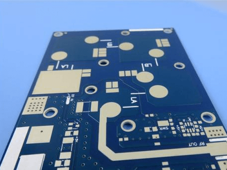
Minimizing RF PCB interference is a critical aspect of designing reliable and efficient radio frequency (RF) printed circuit boards (PCBs). The complexity of RF signals, coupled with the high frequencies at which they operate, makes them particularly susceptible to various forms of interference. Therefore, implementing effective techniques to mitigate these interferences is essential for ensuring optimal performance and functionality of RF circuits.
One of the primary techniques for minimizing RF PCB interference is proper grounding.
A well-designed grounding system can significantly reduce noise and prevent unwanted signal coupling. Ensuring a low-impedance ground path is crucial, as it provides a stable reference point for the RF signals. Utilizing a ground plane, which is a continuous layer of conductive material, can help achieve this. The ground plane should be as large and uninterrupted as possible, covering the entire PCB to provide a uniform ground potential. Additionally, connecting the ground plane to the chassis ground at multiple points can further enhance its effectiveness.
Another important technique involves careful routing of signal traces.
Signal traces should be kept as short and direct as possible to minimize the potential for interference. When routing high-frequency signals, it is advisable to use microstrip or stripline configurations, which provide controlled impedance and reduce signal reflections. Moreover, maintaining adequate spacing between signal traces can prevent crosstalk, a phenomenon where signals from one trace interfere with those on an adjacent trace. This spacing should be determined based on the operating frequency and the characteristics of the PCB material.
Shielding is also a vital method for reducing RF interference.
By enclosing sensitive components and signal traces within a conductive shield, external electromagnetic interference (EMI) can be effectively blocked. This shielding can be implemented using metal enclosures or by incorporating ground planes and vias to create a Faraday cage around critical areas. It is important to ensure that the shield is properly grounded to avoid creating unintended resonant cavities that could exacerbate interference.
In addition to grounding, routing, and shielding, the use of decoupling capacitors is essential for minimizing RF interference.
These capacitors are placed close to the power supply pins of active components to filter out high-frequency noise. Selecting capacitors with appropriate values and low equivalent series resistance (ESR) is crucial for effective decoupling. Furthermore, placing multiple capacitors with different values in parallel can provide a broader frequency range of noise suppression.
Component placement also plays a significant role in minimizing RF interference.
Sensitive components, such as oscillators and amplifiers, should be placed away from noisy elements like power supplies and digital circuits. Grouping components with similar functions together can help reduce the potential for interference. Additionally, maintaining a consistent layout across different PCB layers can prevent signal degradation and ensure signal integrity.
Lastly, the use of proper PCB materials is fundamental in minimizing RF interference.
High-frequency signals require materials with low dielectric loss and stable dielectric constant to maintain signal integrity. Materials such as Rogers or Teflon-based substrates are often preferred for RF applications due to their superior electrical properties. Selecting the right material can significantly impact the overall performance of the RF PCB.
In conclusion, minimizing RF PCB interference requires a comprehensive approach that encompasses grounding, signal routing, shielding, decoupling, component placement, and material selection. By meticulously implementing these techniques, designers can effectively mitigate interference, ensuring the reliable operation of RF circuits. The complexity of RF design necessitates a thorough understanding of these principles to achieve optimal performance and functionality in RF PCBs.

