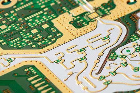
Rf pcb shield
Benefits Of Using RF PCB Shields In Modern Electronics
In the realm of modern electronics, the utilization of RF PCB shields has become increasingly prevalent, driven by the need to enhance device performance and ensure electromagnetic compatibility.
RF PCB shields, or Radio Frequency Printed Circuit Board shields, serve as protective barriers that mitigate the adverse effects of electromagnetic interference (EMI) and radio frequency interference (RFI). These shields are essential in maintaining the integrity of electronic signals, thereby ensuring the reliable operation of various electronic devices.
One of the primary benefits of using RF PCB shields is their ability to significantly reduce EMI and RFI.
In electronic systems, components often emit electromagnetic waves that can interfere with the operation of nearby circuits. This interference can lead to signal degradation, data loss, and even complete system failure. By incorporating RF PCB shields, designers can effectively isolate sensitive components from these disruptive emissions, thereby preserving signal quality and enhancing overall device performance.
Moreover, RF PCB shields contribute to improved signal integrity.
In high-frequency applications, maintaining signal integrity is crucial for accurate data transmission. Without adequate shielding, signals can become distorted due to crosstalk and other forms of interference. RF PCB shields provide a controlled environment that minimizes these disturbances, ensuring that signals remain clear and precise. This is particularly important in applications such as wireless communication, where even minor signal degradation can result in significant performance issues.
In addition to enhancing signal integrity, RF PCB shields also play a vital role in ensuring electromagnetic compatibility (EMC).
EMC is the ability of electronic devices to operate without causing or being affected by unwanted electromagnetic interference. Regulatory bodies impose strict EMC standards to prevent devices from interfering with each other. By incorporating RF PCB shields, manufacturers can design products that comply with these standards, thereby avoiding costly redesigns and ensuring market acceptance.
Furthermore, RF PCB shields offer thermal management benefits.
Electronic components generate heat during operation, and excessive heat can lead to component failure and reduced lifespan. RF PCB shields can be designed to include thermal management features, such as heat sinks or thermal vias, which help dissipate heat away from critical components. This not only enhances the reliability of the device but also allows for higher power densities and more compact designs.
Another advantage of RF PCB shields is their contribution to miniaturization.
As consumer demand for smaller, more portable devices continues to grow, the need for compact and efficient electronic designs becomes paramount. RF PCB shields enable designers to pack more functionality into smaller spaces by providing effective EMI and RFI protection without the need for bulky external shielding solutions. This facilitates the development of sleek, lightweight devices that meet modern consumer expectations.
Additionally, RF PCB shields can enhance the durability and longevity of electronic devices.
By protecting sensitive components from external electromagnetic interference, these shields help prevent premature wear and tear. This is particularly important in harsh environments where devices are exposed to high levels of EMI, such as industrial settings or military applications. The added protection provided by RF PCB shields ensures that devices remain operational and reliable over extended periods.
In conclusion, the benefits of using RF PCB shields in modern electronics are manifold. From reducing EMI and RFI to improving signal integrity, ensuring EMC compliance, aiding in thermal management, facilitating miniaturization, and enhancing device durability, RF PCB shields are indispensable in the design and development of contemporary electronic systems. As technology continues to advance, the importance of these shields in maintaining the performance and reliability of electronic devices will only continue to grow.
Design Considerations For Effective RF PCB Shielding
Designing effective RF PCB shielding is a critical aspect of ensuring optimal performance and reliability in electronic devices. The primary objective of RF shielding is to prevent electromagnetic interference (EMI) from affecting the functionality of sensitive components on a printed circuit board (PCB). To achieve this, several design considerations must be meticulously addressed.
Firstly, the choice of materials for the shield is paramount.
Conductive materials such as copper, aluminum, and specialized alloys are commonly used due to their excellent EMI attenuation properties. The thickness of the shielding material also plays a crucial role; it must be sufficient to block unwanted signals without adding excessive weight or bulk to the device. Additionally, the material should be compatible with the PCB’s thermal and mechanical requirements to ensure long-term reliability.
Transitioning to the layout of the PCB, the placement of the shield is another vital consideration.
The shield should be strategically positioned to cover the most sensitive components and circuits. This often involves creating a Faraday cage around critical areas, which can effectively block external electromagnetic fields. However, it is essential to ensure that the shield does not interfere with the normal operation of the components it is meant to protect. This requires careful planning and simulation during the design phase.
Moreover, the grounding of the shield is a critical factor that cannot be overlooked.
A well-grounded shield can significantly enhance its effectiveness. The shield should be connected to a low-impedance ground plane to provide a clear path for the unwanted signals to dissipate. This connection must be as short and direct as possible to minimize inductive and resistive losses. Additionally, multiple grounding points can be used to further improve the shield’s performance, especially in high-frequency applications.
In addition to grounding, the design of the PCB traces and components must be considered.
High-frequency signals can easily couple into adjacent traces, leading to crosstalk and signal degradation. To mitigate this, designers should use controlled impedance traces and maintain adequate spacing between high-speed signals and sensitive analog circuits. Furthermore, the use of differential signaling can help reduce susceptibility to EMI by ensuring that any interference affects both lines equally, thereby canceling out the noise.
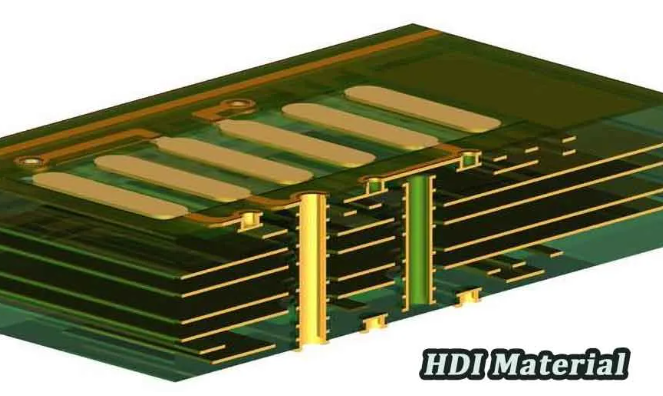
Another important aspect is the use of vias and stitching techniques.
Vias can be used to connect the shield to the ground plane, providing multiple paths for the EMI to be diverted. Stitching vias, placed at regular intervals along the perimeter of the shield, can enhance its effectiveness by preventing high-frequency signals from leaking through gaps. This technique is particularly useful in applications where space constraints limit the size of the shield.
Thermal management is also a crucial consideration in RF PCB shielding design.
The shield can act as a thermal barrier, potentially leading to overheating of the components it protects. To address this, designers can incorporate thermal vias and heat sinks to dissipate heat effectively. Additionally, the use of thermally conductive materials for the shield can help manage heat while maintaining EMI protection.
Finally, it is essential to consider the manufacturability and cost of the RF shield.
While advanced materials and techniques can offer superior performance, they may also increase the complexity and cost of production. Therefore, a balance must be struck between performance requirements and practical constraints.
In conclusion, effective RF PCB shielding requires a comprehensive approach that considers material selection, layout, grounding, trace design, via placement, thermal management, and manufacturability. By addressing these factors, designers can create robust and reliable electronic devices that perform optimally in the presence of electromagnetic interference.
Common Materials Used In RF PCB Shield Construction
In the realm of radio frequency (RF) technology, the construction of printed circuit boards (PCBs) necessitates meticulous attention to detail, particularly when it comes to shielding. RF PCB shields are essential components designed to protect sensitive electronic circuits from electromagnetic interference (EMI) and radio frequency interference (RFI). The effectiveness of these shields largely depends on the materials used in their construction. Understanding the common materials employed in RF PCB shield construction is crucial for ensuring optimal performance and reliability.
One of the most prevalent materials used in RF PCB shield construction is copper. Copper is highly favored due to its excellent electrical conductivity and superior shielding effectiveness. Its ability to attenuate electromagnetic waves makes it an ideal choice for creating barriers that prevent unwanted interference. Additionally, copper’s malleability allows for easy fabrication into various shapes and sizes, accommodating the diverse design requirements of RF PCBs. However, copper is prone to oxidation, which can degrade its performance over time. To mitigate this issue, copper shields are often coated with a layer of tin or nickel, enhancing their durability and resistance to corrosion.
Transitioning from copper, another commonly used material is aluminum. Aluminum is lightweight and offers good conductivity, making it a suitable alternative to copper in certain applications. Its lower density compared to copper can be advantageous in designs where weight is a critical factor. Moreover, aluminum is cost-effective, providing a balance between performance and budget considerations. Despite these benefits, aluminum’s conductivity is not as high as copper’s, which may limit its effectiveness in some high-frequency applications. To address this, aluminum shields are sometimes anodized or treated with conductive coatings to improve their performance.
In addition to metals, conductive elastomers are also employed in RF PCB shield construction. These materials consist of elastomeric compounds embedded with conductive particles, such as silver or nickel. Conductive elastomers offer flexibility and can conform to irregular surfaces, providing a reliable seal against EMI and RFI. Their ability to maintain conductivity while being compressed makes them ideal for applications requiring frequent assembly and disassembly. However, the cost of conductive elastomers can be higher than that of traditional metal shields, which may be a consideration in large-scale production.
Furthermore, composite materials are gaining traction in RF PCB shield construction. These materials combine the properties of different substances to achieve enhanced performance characteristics. For instance, metal-coated fabrics or foils laminated with insulating layers can provide excellent shielding effectiveness while maintaining flexibility and lightweight properties. Composites can be tailored to specific application needs, offering a versatile solution for complex RF PCB designs. Nevertheless, the manufacturing process for composite materials can be more intricate, potentially increasing production time and costs.
Lastly, it is important to mention the role of ferrites in RF PCB shielding. Ferrites are ceramic compounds that exhibit magnetic properties, making them effective at absorbing high-frequency electromagnetic waves. They are often used in conjunction with other shielding materials to enhance overall performance. Ferrite beads or tiles can be strategically placed on PCBs to suppress EMI and RFI, particularly in high-frequency circuits. However, the brittleness of ferrites requires careful handling during assembly to prevent damage.
In conclusion, the selection of materials for RF PCB shield construction is a critical factor that influences the performance and reliability of electronic devices. Copper, aluminum, conductive elastomers, composite materials, and ferrites each offer unique advantages and limitations. By understanding the properties and applications of these materials, designers can make informed decisions to optimize the shielding effectiveness of RF PCBs, ensuring the integrity of sensitive electronic circuits in the presence of electromagnetic interference.
Troubleshooting RF Interference With PCB Shielding Techniques
In the realm of modern electronics, the proliferation of wireless communication devices has necessitated the development of effective techniques to mitigate radio frequency (RF) interference.
One of the most critical methods employed in this endeavor is the use of RF PCB shielding.
This technique involves the strategic placement of conductive materials around sensitive components on a printed circuit board (PCB) to prevent unwanted electromagnetic interference (EMI) from disrupting the device’s functionality. Understanding the intricacies of RF PCB shielding is essential for engineers and designers aiming to ensure the reliability and performance of their electronic systems.
To begin with, RF interference can originate from various sources, including external devices, internal components, and even the PCB itself.
External sources such as nearby electronic devices, power lines, and wireless communication signals can introduce unwanted noise into the system. Internally, components like oscillators, microprocessors, and switching power supplies can generate significant RF emissions. Additionally, the PCB’s layout, trace routing, and grounding can inadvertently create pathways for EMI to propagate. Consequently, addressing these potential sources of interference is paramount in the design phase.
One of the primary techniques for mitigating RF interference is the implementation of shielding enclosures.
These enclosures are typically made from conductive materials such as copper, aluminum, or specialized alloys, which effectively block or attenuate electromagnetic waves. By enclosing sensitive components within these shields, engineers can create a barrier that prevents external RF signals from penetrating and internal signals from escaping. This approach is particularly useful in applications where high-frequency signals are prevalent, such as in wireless communication devices and high-speed digital circuits.
In addition to shielding enclosures, PCB designers often employ ground planes and ground traces to enhance the effectiveness of RF shielding.
A ground plane is a large area of copper on the PCB that serves as a reference point for all signals and provides a low-impedance path for return currents. By strategically placing ground planes beneath critical components and traces, designers can minimize the potential for EMI to couple into or out of the circuit. Furthermore, ground traces can be used to connect different sections of the ground plane, ensuring a continuous and effective shield.
Another crucial aspect of RF PCB shielding is the careful routing of signal traces.
High-frequency signals are particularly susceptible to interference, and improper trace routing can exacerbate this issue. To mitigate this, designers should keep high-speed signal traces as short as possible and avoid running them parallel to each other, which can create crosstalk. Additionally, using differential pairs for high-speed signals can help cancel out common-mode noise, further reducing the potential for interference.
Moreover, the selection of appropriate materials for the PCB substrate can significantly impact the effectiveness of RF shielding.
Materials with low dielectric constants and low loss tangents are preferred, as they minimize signal attenuation and dispersion. Additionally, using materials with high thermal conductivity can help dissipate heat generated by high-frequency components, ensuring the long-term reliability of the device.
In conclusion, troubleshooting RF interference with PCB shielding techniques is a multifaceted process that requires a comprehensive understanding of electromagnetic principles and meticulous attention to design details. By employing shielding enclosures, ground planes, careful trace routing, and selecting suitable materials, engineers can effectively mitigate RF interference and ensure the optimal performance of their electronic systems. As wireless communication continues to evolve, the importance of robust RF PCB shielding techniques will only grow, underscoring the need for ongoing innovation and expertise in this critical field.