Rf pcb testing
Importance Of RF PCB Testing In Modern Electronics
In the rapidly evolving landscape of modern electronics, the importance of RF PCB (Radio Frequency Printed Circuit Board) testing cannot be overstated. As devices become increasingly sophisticated and interconnected, ensuring the reliability and performance of RF PCBs is paramount.
These components are integral to a wide array of applications, from telecommunications and medical devices to automotive systems and consumer electronics. Consequently, rigorous testing protocols are essential to maintain the integrity and functionality of these critical components.
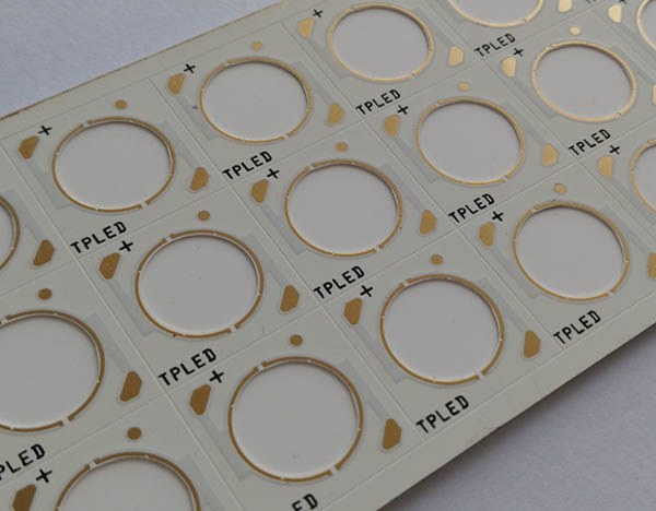
To begin with, RF PCBs are designed to handle high-frequency signals, which are inherently more susceptible to interference and signal degradation.
This makes them fundamentally different from standard PCBs, necessitating specialized testing methods. The primary objective of RF PCB testing is to verify that the board can transmit and receive signals with minimal loss and distortion. This is crucial because any deviation can lead to significant performance issues, such as poor signal quality, reduced range, and increased error rates. Therefore, comprehensive testing ensures that the RF PCB meets the stringent requirements of its intended application.
Moreover, the complexity of RF PCB designs further underscores the need for meticulous testing.
These boards often incorporate intricate layouts, including multiple layers and precise impedance control, to manage high-frequency signals effectively. Any manufacturing defects, such as misaligned traces or improper soldering, can severely impact the board’s performance. Through various testing techniques, such as Time Domain Reflectometry (TDR) and Vector Network Analysis (VNA), engineers can identify and rectify these issues before the product reaches the market. This not only enhances the reliability of the device but also reduces the likelihood of costly recalls and repairs.
In addition to ensuring performance, RF PCB testing plays a critical role in compliance with industry standards and regulations.
Regulatory bodies, such as the Federal Communications Commission (FCC) in the United States, impose strict guidelines on the electromagnetic compatibility (EMC) and electromagnetic interference (EMI) of electronic devices. Non-compliance can result in hefty fines and market restrictions. By conducting thorough RF PCB testing, manufacturers can certify that their products adhere to these standards, thereby avoiding legal complications and ensuring smooth market entry.
Furthermore, the advent of emerging technologies, such as 5G and the Internet of Things (IoT), has heightened the demand for high-performance RF PCBs.
These technologies require boards that can operate at even higher frequencies and support greater data rates. As a result, the testing processes must evolve to address these new challenges. Advanced testing methodologies, including over-the-air (OTA) testing and millimeter-wave (mmWave) testing, are now being employed to validate the performance of next-generation RF PCBs. This continuous innovation in testing techniques is vital to keep pace with the rapid advancements in technology.
Lastly, it is important to recognize that RF PCB testing is not a one-time process but an ongoing necessity throughout the product lifecycle.
From the initial design phase to mass production and field deployment, continuous testing ensures that the RF PCB maintains its performance and reliability. This iterative approach allows for early detection of potential issues, enabling timely interventions and minimizing the risk of failure in real-world applications.
In conclusion, the importance of RF PCB testing in modern electronics is multifaceted, encompassing performance verification, compliance with regulatory standards, adaptation to emerging technologies, and ongoing quality assurance. As the demand for high-frequency, high-performance devices continues to grow, the role of RF PCB testing will only become more critical. By investing in robust testing protocols, manufacturers can ensure the success and longevity of their products in an increasingly competitive market.
Techniques For Effective RF PCB Testing
Effective RF PCB testing is crucial for ensuring the reliability and performance of radio frequency printed circuit boards, which are integral to a wide range of applications, from telecommunications to consumer electronics. To achieve accurate and reliable results, several techniques must be employed, each addressing different aspects of the testing process. Understanding these techniques and their implementation can significantly enhance the quality and functionality of RF PCBs.
One of the primary techniques for effective RF PCB testing is the use of vector network analyzers (VNAs).
VNAs are essential tools for measuring the electrical performance of RF circuits, providing detailed information on parameters such as return loss, insertion loss, and impedance. By connecting the VNA to the RF PCB, engineers can obtain a comprehensive understanding of how the board will perform in real-world conditions. This data is invaluable for identifying any discrepancies or issues that may affect the board’s performance, allowing for timely corrections and optimizations.
In addition to VNAs, time-domain reflectometry (TDR) is another critical technique used in RF PCB testing.
TDR involves sending a fast electrical pulse through the PCB and measuring the reflections that occur due to impedance mismatches. These reflections can indicate the presence of defects such as open circuits, short circuits, or discontinuities in the transmission lines. By analyzing the TDR data, engineers can pinpoint the exact location and nature of these defects, facilitating targeted repairs and improvements.
Moreover, signal integrity testing plays a vital role in ensuring the proper functioning of RF PCBs.
Signal integrity testing involves evaluating the quality of the signals transmitted through the PCB, focusing on parameters such as signal attenuation, crosstalk, and jitter. Techniques such as eye diagram analysis and bit error rate testing are commonly used to assess signal integrity. Eye diagrams provide a visual representation of the signal quality, highlighting any distortions or noise that may affect performance. Bit error rate testing, on the other hand, quantifies the number of errors in a transmitted data stream, offering a clear metric for evaluating signal integrity.
Thermal testing is another important aspect of RF PCB testing, as temperature variations can significantly impact the performance of RF circuits.
Thermal testing involves subjecting the PCB to different temperature conditions and monitoring its behavior. Techniques such as thermal cycling and thermal imaging are used to identify any thermal-related issues, such as component overheating or thermal expansion. By addressing these issues, engineers can ensure that the RF PCB will operate reliably under various environmental conditions.
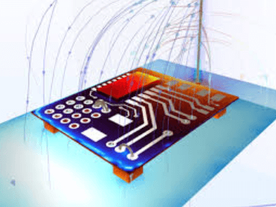
Furthermore, electromagnetic compatibility (EMC) testing is essential for ensuring that RF PCBs do not interfere with other electronic devices and comply with regulatory standards. EMC testing involves measuring the electromagnetic emissions from the PCB and assessing its susceptibility to external electromagnetic interference. Techniques such as radiated emissions testing and conducted emissions testing are used to evaluate the PCB’s EMC performance. By identifying and mitigating any EMC issues, engineers can ensure that the RF PCB will function correctly in its intended application without causing or being affected by electromagnetic interference.
In conclusion, effective RF PCB testing requires a comprehensive approach that incorporates various techniques to evaluate different aspects of the board’s performance. By utilizing tools such as vector network analyzers, time-domain reflectometry, signal integrity testing, thermal testing, and electromagnetic compatibility testing, engineers can ensure that RF PCBs meet the necessary standards and perform reliably in their intended applications. These techniques, when applied correctly, provide valuable insights into the PCB’s behavior, enabling timely identification and resolution of potential issues, ultimately leading to the development of high-quality RF PCBs.
Common Challenges In RF PCB Testing And How To Overcome Them
RF PCB testing is a critical phase in the development and production of radio frequency printed circuit boards, ensuring that these components meet stringent performance and reliability standards. However, this process is fraught with numerous challenges that can impede the accuracy and efficiency of testing. Understanding these common challenges and implementing strategies to overcome them is essential for achieving optimal results.
One of the primary challenges in RF PCB testing is signal integrity.
High-frequency signals are particularly susceptible to interference and loss, which can distort the results of the tests. To mitigate this issue, it is crucial to use high-quality test equipment and maintain a controlled testing environment. Shielding the test setup from external electromagnetic interference (EMI) and using proper grounding techniques can significantly enhance signal integrity. Additionally, employing advanced signal processing algorithms can help in distinguishing the actual signal from noise, thereby improving the accuracy of the test results.
Another significant challenge is the complexity of RF PCB designs.
Modern RF PCBs often incorporate multiple layers and intricate layouts, making it difficult to access all the test points. This complexity can lead to incomplete testing and overlooked defects. To address this, designers should consider incorporating test points and vias during the design phase, facilitating easier access during testing. Automated test equipment (ATE) can also be employed to handle complex testing procedures, ensuring comprehensive coverage and reducing the likelihood of human error.
Thermal management is another critical aspect that poses challenges during RF PCB testing.
High-frequency components tend to generate substantial heat, which can affect their performance and reliability. Effective thermal management strategies, such as using heat sinks, thermal vias, and proper ventilation, are essential to maintain the components within their optimal temperature range. During testing, it is important to monitor the temperature of the components and the PCB to ensure that they do not exceed their specified limits. Thermal imaging cameras and temperature sensors can be used to detect hotspots and ensure effective heat dissipation.
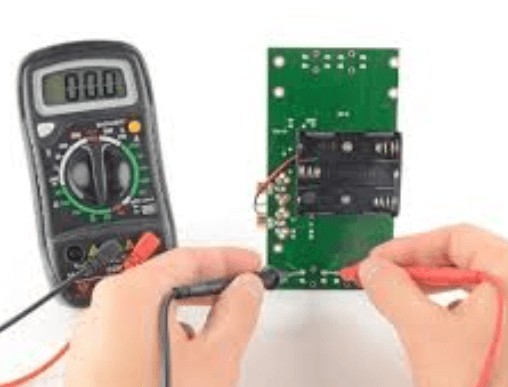
Calibration and measurement accuracy are also pivotal in RF PCB testing.
Inaccurate calibration of test equipment can lead to erroneous results, compromising the reliability of the tests. Regular calibration of test instruments, following manufacturer guidelines, is essential to maintain measurement accuracy. Additionally, using precision measurement tools and techniques can help in obtaining reliable data. Cross-referencing measurements with known standards and conducting repeatability tests can further enhance the credibility of the test results.
Moreover, the miniaturization of RF components presents another layer of difficulty.
As components become smaller, the precision required for testing increases. Handling and testing these tiny components without causing damage requires specialized equipment and techniques. Employing micro-probing techniques and using high-resolution microscopes can aid in accurately testing these miniature components. Furthermore, training personnel in handling and testing small components can reduce the risk of damage and improve the overall testing process.
In conclusion, RF PCB testing is a complex and challenging process that requires meticulous attention to detail and the implementation of robust strategies to overcome common obstacles. By addressing issues related to signal integrity, design complexity, thermal management, calibration accuracy, and component miniaturization, manufacturers can ensure that their RF PCBs meet the highest standards of performance and reliability. Adopting advanced testing technologies and maintaining a controlled testing environment are key to achieving accurate and reliable test results, ultimately leading to the successful deployment of RF PCBs in various applications.
Innovations In RF PCB Testing Equipment And Methods
The field of RF PCB (Radio Frequency Printed Circuit Board) testing has witnessed significant advancements in recent years, driven by the increasing complexity and performance demands of modern electronic devices. Innovations in RF PCB testing equipment and methods are crucial for ensuring the reliability and efficiency of these high-frequency circuits, which are integral to applications ranging from telecommunications to aerospace.
One of the most notable innovations in RF PCB testing is the development of advanced vector network analyzers (VNAs).
These sophisticated instruments are capable of measuring the complex impedance and scattering parameters of RF circuits with unprecedented accuracy. Modern VNAs offer enhanced frequency ranges, higher dynamic ranges, and improved calibration techniques, enabling engineers to perform more precise and comprehensive analyses of RF PCBs. The integration of automated calibration routines and error correction algorithms further enhances the reliability of measurements, reducing the potential for human error and ensuring consistent results.
In addition to VNAs, time-domain reflectometry (TDR) has emerged as a powerful method for characterizing RF PCBs.
TDR techniques involve sending a fast-rise-time pulse down a transmission line and observing the reflections caused by impedance discontinuities. This method provides valuable insights into the integrity of signal paths, identifying issues such as open circuits, short circuits, and impedance mismatches. Recent advancements in TDR technology have led to the development of high-resolution TDR instruments capable of detecting even the smallest anomalies in RF circuits, thereby improving the overall quality and performance of RF PCBs.
Another significant innovation in RF PCB testing is the use of non-contact testing methods.
Traditional contact-based testing methods, such as probe-based measurements, can introduce parasitic effects and potentially damage delicate RF components. Non-contact methods, such as near-field scanning and electromagnetic field mapping, offer a solution to these challenges. Near-field scanning involves measuring the electromagnetic fields in close proximity to the PCB surface, providing detailed information about the distribution of RF signals and identifying areas of signal leakage or interference. Electromagnetic field mapping, on the other hand, uses advanced sensors to create a three-dimensional representation of the electromagnetic environment around the PCB, enabling engineers to visualize and analyze the behavior of RF signals in real-time.
The integration of machine learning and artificial intelligence (AI) into RF PCB testing is another groundbreaking development.
Machine learning algorithms can analyze vast amounts of test data, identifying patterns and correlations that may not be immediately apparent to human observers. This capability allows for the early detection of potential issues and the optimization of RF PCB designs. AI-driven testing systems can also adapt to changing conditions and continuously improve their performance, leading to more efficient and accurate testing processes.
Furthermore, the advent of modular and scalable testing platforms has revolutionized the way RF PCBs are tested.
These platforms allow for the customization of testing setups to meet specific requirements, enabling engineers to perform a wide range of tests using a single system. Modular platforms also facilitate the integration of new testing technologies as they become available, ensuring that testing capabilities remain up-to-date with the latest advancements in the field.
In conclusion, the innovations in RF PCB testing equipment and methods have significantly enhanced the ability of engineers to ensure the performance and reliability of high-frequency circuits. Advanced vector network analyzers, time-domain reflectometry, non-contact testing methods, machine learning, and modular testing platforms represent just a few of the groundbreaking developments that are shaping the future of RF PCB testing. As technology continues to evolve, these innovations will play a crucial role in meeting the growing demands of modern electronic applications, driving further advancements in the field.