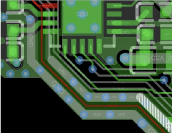
Rf pcb via diameter
Importance Of Via Diameter In RF PCB Design
In the realm of Radio Frequency (RF) Printed Circuit Board (PCB) design, the importance of via diameter cannot be overstated. Vias, which are small conductive pathways that connect different layers of a PCB, play a crucial role in ensuring signal integrity and overall performance. The diameter of these vias is a critical parameter that influences various aspects of the PCB, including signal transmission, thermal management, and mechanical stability.
To begin with, the diameter of a via directly impacts the impedance of the signal path.
In RF applications, maintaining a consistent impedance is essential to minimize signal reflection and loss. A via with an inappropriate diameter can introduce impedance discontinuities, leading to signal degradation. This is particularly problematic in high-frequency circuits where even minor impedance mismatches can result in significant performance issues. Therefore, selecting the correct via diameter is vital to ensure that the signal path remains as uniform as possible, thereby preserving signal integrity.
Moreover, the via diameter affects the inductance and capacitance of the PCB.
Smaller vias tend to have higher inductance, which can be detrimental in RF circuits where low inductance is often required to maintain high-speed signal transmission. Conversely, larger vias can introduce unwanted capacitance, which can also degrade signal quality. Striking a balance between these two factors is essential for optimizing the performance of the RF PCB. Designers must carefully consider the trade-offs and select a via diameter that minimizes both inductance and capacitance to achieve the desired electrical characteristics.
In addition to electrical considerations, thermal management is another critical aspect influenced by via diameter.
Vias are often used to conduct heat away from critical components, thereby preventing overheating and ensuring reliable operation. Larger vias can dissipate heat more effectively due to their increased cross-sectional area, which allows for better thermal conductivity. However, excessively large vias can compromise the mechanical integrity of the PCB and occupy valuable real estate, which is often at a premium in compact RF designs. Therefore, designers must choose a via diameter that provides adequate thermal management without compromising the structural integrity or layout efficiency of the PCB.
Furthermore, the manufacturing process imposes certain constraints on via diameter.
The capabilities of the fabrication facility, including the precision of drilling equipment and the quality of plating processes, determine the minimum and maximum via sizes that can be reliably produced. Designers must work within these constraints to ensure that the vias can be manufactured to the required specifications. This often involves close collaboration with the PCB manufacturer to understand their capabilities and limitations, thereby ensuring that the design can be successfully realized.
Lastly, the via diameter also has implications for the mechanical stability of the PCB.
Vias that are too small may be prone to failure under mechanical stress, such as during assembly or operation in harsh environments. On the other hand, excessively large vias can weaken the PCB structure, making it more susceptible to damage. Therefore, selecting an appropriate via diameter is essential to ensure that the PCB can withstand the mechanical demands of its intended application.
In conclusion, the diameter of vias in RF PCB design is a critical parameter that influences signal integrity, thermal management, manufacturability, and mechanical stability. Designers must carefully consider these factors and strike a balance to optimize the performance and reliability of the PCB. By understanding the importance of via diameter and making informed decisions, designers can ensure that their RF circuits meet the stringent requirements of modern applications.
Optimizing Via Diameter For High-Frequency Performance
In the realm of high-frequency printed circuit board (PCB) design, optimizing via diameter is a critical consideration that can significantly impact the overall performance of the radio frequency (RF) circuitry. Vias, which are the conductive pathways that connect different layers of a PCB, play a pivotal role in ensuring signal integrity and minimizing losses. Therefore, understanding the implications of via diameter on high-frequency performance is essential for engineers aiming to achieve optimal functionality in their designs.
To begin with, the diameter of a via influences several key parameters, including inductance, capacitance, and resistance.
At high frequencies, these parameters become increasingly significant due to the skin effect, where the current tends to flow on the surface of the conductor, thereby increasing the effective resistance. A larger via diameter can reduce the inductive reactance, which is beneficial for maintaining signal integrity. However, it is also important to consider the trade-offs involved. While a larger via diameter can lower inductance, it may also increase the parasitic capacitance, which can adversely affect the signal quality by introducing unwanted coupling between different signal paths.
Moreover, the aspect ratio of the via, defined as the ratio of the via length to its diameter, is another crucial factor.
A high aspect ratio can lead to manufacturing challenges and reliability issues, such as incomplete plating or voids within the via. Consequently, designers must strike a balance between achieving the desired electrical performance and ensuring manufacturability. Advanced fabrication techniques, such as laser drilling and microvias, offer solutions to mitigate these challenges by enabling the creation of smaller, more precise vias with lower aspect ratios.
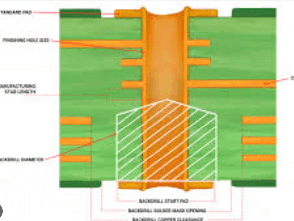
Transitioning to the impact of via diameter on signal integrity, it is essential to consider the role of via stubs.
Via stubs are the unused portions of vias that extend beyond the signal layer, acting as resonant structures that can cause signal reflections and degradation. To minimize the adverse effects of via stubs, techniques such as back-drilling or using blind and buried vias can be employed. These methods effectively remove or reduce the length of the via stubs, thereby enhancing the high-frequency performance of the PCB.
Furthermore, the choice of via diameter is also influenced by the type of signal being transmitted.
For instance, differential signals, which are commonly used in high-speed digital and RF applications, require careful matching of via diameters to ensure balanced impedance and minimize skew. In contrast, single-ended signals may have different requirements, necessitating a tailored approach to via diameter selection.
In addition to electrical considerations, thermal management is another aspect where via diameter plays a significant role.
Vias are often used as thermal vias to dissipate heat from high-power components. A larger via diameter can enhance thermal conductivity, thereby improving the heat dissipation capabilities of the PCB. However, this must be balanced against the potential impact on the electrical performance, as previously discussed.
In conclusion, optimizing via diameter for high-frequency performance is a multifaceted challenge that requires a comprehensive understanding of the interplay between electrical, thermal, and manufacturing considerations. By carefully evaluating the trade-offs and employing advanced design and fabrication techniques, engineers can achieve the desired balance, ensuring that their RF PCBs deliver optimal performance in demanding high-frequency applications.
Common Mistakes In RF PCB Via Diameter Selection
Selecting the appropriate via diameter in RF PCB design is a critical aspect that can significantly impact the performance and reliability of the final product. One common mistake in RF PCB via diameter selection is underestimating the importance of via size in relation to signal integrity. Smaller vias can introduce higher inductance, which can degrade signal quality, especially at higher frequencies. Conversely, larger vias may reduce inductance but can also increase parasitic capacitance, leading to signal distortion. Therefore, striking a balance between via size and the electrical characteristics of the circuit is essential.
Another frequent error is neglecting the thermal management implications of via diameter.
Vias play a crucial role in heat dissipation, particularly in high-power RF applications. Insufficient via diameter can lead to inadequate thermal conduction, causing hotspots and potentially damaging the PCB and its components. Designers must consider the thermal conductivity requirements and ensure that the via diameter is sufficient to facilitate effective heat transfer.
Additionally, mechanical reliability is often overlooked when selecting via diameter.
Smaller vias are more susceptible to mechanical stress and can be prone to cracking, especially during thermal cycling. This can compromise the structural integrity of the PCB and lead to premature failure. On the other hand, larger vias may provide better mechanical stability but can also occupy more space, which might not be feasible in densely packed designs. Therefore, it is crucial to evaluate the mechanical robustness of the vias in conjunction with their electrical and thermal performance.
Furthermore, manufacturing constraints can pose significant challenges in via diameter selection.
The capabilities of the PCB fabrication process must be taken into account, as not all manufacturers can produce vias of extremely small or large diameters with high precision. Designers should collaborate closely with manufacturers to understand their limitations and ensure that the chosen via diameters are within the feasible range. This collaboration can help avoid costly redesigns and production delays.
Another aspect that is often disregarded is the impact of via diameter on impedance control.
In RF circuits, maintaining consistent impedance is vital for minimizing signal reflection and loss. Vias with inappropriate diameters can disrupt the impedance profile, leading to signal integrity issues. It is essential to perform thorough impedance calculations and simulations to determine the optimal via diameter that aligns with the desired impedance characteristics of the circuit.
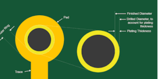
Moreover, the aspect of via filling and plating should not be ignored.
Inadequate via filling can result in voids, which can affect both the electrical and thermal performance of the vias. Proper via filling techniques, such as copper filling or conductive epoxy, should be employed to ensure reliable via performance. Additionally, the plating thickness must be sufficient to provide good electrical conductivity and mechanical strength.
In conclusion, selecting the correct via diameter in RF PCB design is a multifaceted process that requires careful consideration of various factors, including signal integrity, thermal management, mechanical reliability, manufacturing constraints, impedance control, and via filling. By addressing these common mistakes and adopting a holistic approach to via diameter selection, designers can enhance the performance, reliability, and manufacturability of their RF PCBs.
Advanced Techniques For Via Diameter Calculation In RF PCBs
In the realm of radio frequency (RF) printed circuit boards (PCBs), the precision of via diameter calculation is paramount. Vias, which are the conductive pathways that connect different layers of a PCB, play a crucial role in maintaining signal integrity and minimizing losses. As RF circuits operate at high frequencies, even minor discrepancies in via dimensions can lead to significant performance degradation. Therefore, advanced techniques for via diameter calculation are essential to ensure optimal functionality.
One of the primary considerations in via diameter calculation is the frequency of the signal.
At higher frequencies, the skin effect becomes more pronounced, causing the current to flow primarily on the surface of the conductor. This phenomenon necessitates a careful balance between the via diameter and the plating thickness to minimize resistance and inductance. To achieve this, designers often employ electromagnetic simulation tools that model the behavior of RF signals within the PCB structure. These tools can provide insights into the optimal via dimensions by simulating various scenarios and analyzing the resulting signal integrity.
Another critical factor is the dielectric material used in the PCB.
Different materials exhibit varying dielectric constants and loss tangents, which can affect the propagation of RF signals. When calculating via diameters, it is essential to consider the dielectric properties to ensure that the vias do not introduce unwanted impedance mismatches. Advanced techniques involve the use of material characterization data and sophisticated algorithms to predict the impact of the dielectric on via performance. By incorporating these factors into the calculation process, designers can achieve more accurate and reliable results.
Thermal management is also a significant concern in RF PCBs, as high-frequency signals can generate substantial heat.
The via diameter must be calculated to facilitate efficient heat dissipation while maintaining electrical performance. Techniques such as thermal simulation and finite element analysis (FEA) are employed to model the thermal behavior of the PCB and optimize the via dimensions accordingly. These simulations help identify potential hotspots and ensure that the vias can handle the thermal load without compromising signal integrity.
Moreover, manufacturing tolerances must be taken into account when calculating via diameters.
The fabrication process can introduce variations in via dimensions, which can affect the overall performance of the RF PCB. Advanced techniques involve statistical analysis and process capability studies to understand the potential variations and incorporate them into the design. By accounting for these tolerances, designers can ensure that the vias remain within acceptable limits and maintain consistent performance across different manufacturing batches.
Additionally, the aspect ratio of the via, which is the ratio of its length to its diameter, plays a crucial role in determining its electrical and thermal properties.
A higher aspect ratio can lead to increased inductance and resistance, which can degrade signal quality. Advanced techniques involve optimizing the aspect ratio by adjusting the via diameter and the PCB stack-up configuration. This optimization process often requires iterative simulations and prototyping to achieve the desired balance between electrical performance and manufacturability.
In conclusion, the calculation of via diameter in RF PCBs is a complex process that requires a thorough understanding of various factors, including signal frequency, dielectric properties, thermal management, manufacturing tolerances, and aspect ratio. Advanced techniques such as electromagnetic simulation, thermal analysis, and statistical modeling are essential to achieve accurate and reliable results. By employing these techniques, designers can ensure that the vias in RF PCBs are optimized for performance, reliability, and manufacturability, ultimately leading to superior RF circuit performance.