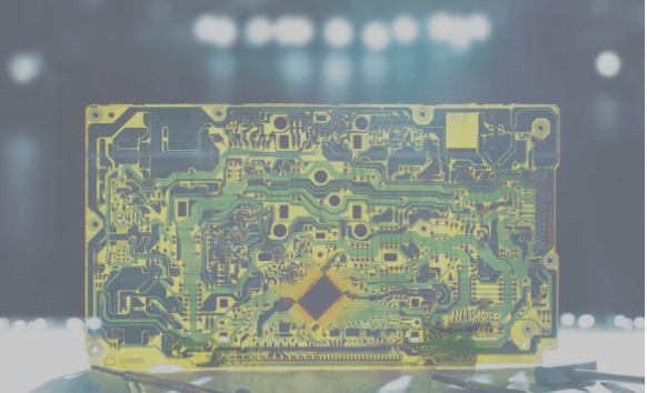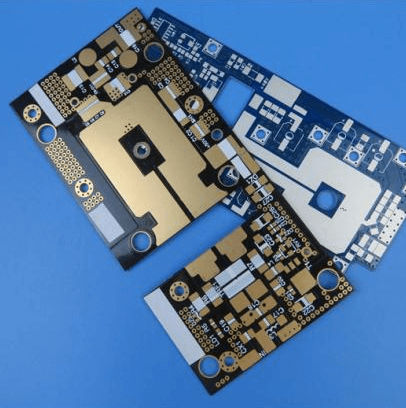
Rf shield box pcb
Design Considerations for RF Shield Box PCB
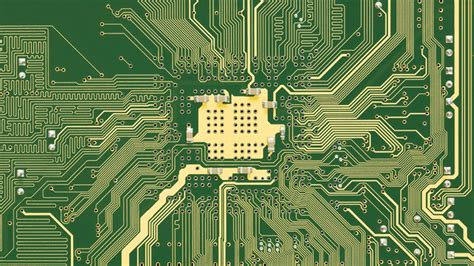
When designing a printed circuit board (PCB) for an RF shield box, several critical considerations must be taken into account to ensure optimal performance and functionality. The primary objective of an RF shield box is to isolate sensitive electronic components from external electromagnetic interference (EMI) and to prevent the emission of potentially disruptive signals. Therefore, the design of the PCB within this enclosure is paramount to achieving these goals.
To begin with, the layout of the PCB is crucial.
Proper component placement can significantly reduce the risk of EMI. High-frequency components should be positioned as far away from sensitive analog circuits as possible. Additionally, it is advisable to place components that generate significant noise, such as oscillators and switching regulators, near the power input to confine their noise within a limited area. This strategic placement minimizes the potential for interference with other components on the board.
Moreover, the use of ground planes is essential in RF PCB design.
A continuous ground plane can provide a low-impedance path for return currents, thereby reducing the potential for EMI. It is important to ensure that the ground plane is as unbroken as possible, avoiding unnecessary splits or gaps. When splits are unavoidable, they should be carefully managed to prevent the creation of unintended antennas that could radiate or pick up unwanted signals.
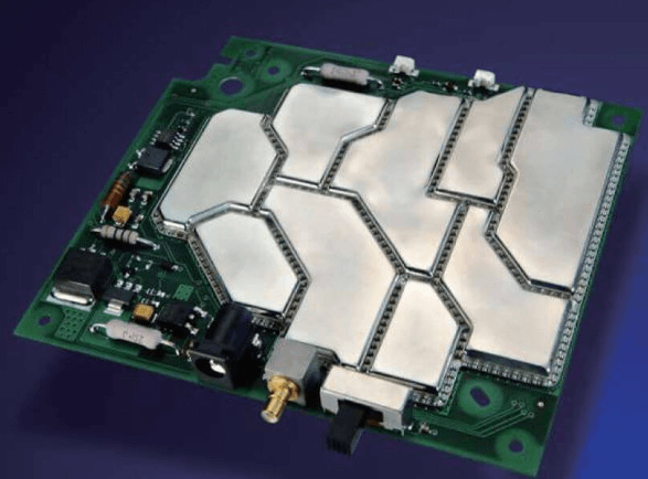
In addition to ground planes, the implementation of proper shielding techniques is vital.
Shielding can be achieved through the use of metal enclosures or by incorporating shielded traces and vias. Metal enclosures can provide a physical barrier against EMI, while shielded traces and vias can help to contain and direct signals within the PCB. It is also beneficial to use vias to connect the ground planes on different layers of the PCB, creating a more robust grounding system.
Transitioning to the topic of signal integrity, it is important to consider the impedance of the traces on the PCB.
Impedance matching is critical in RF design to ensure that signals are transmitted with minimal reflection and loss. This can be achieved by carefully controlling the width and spacing of the traces, as well as the dielectric properties of the PCB material. Utilizing controlled impedance traces can help to maintain signal integrity and reduce the risk of signal degradation.
Furthermore, power supply decoupling is another key consideration.
Decoupling capacitors should be placed as close as possible to the power pins of active components to filter out high-frequency noise. This practice helps to maintain a stable power supply and reduces the potential for noise to propagate through the power distribution network.
Thermal management is also an important aspect of RF PCB design.
High-frequency components can generate significant amounts of heat, which can affect the performance and reliability of the PCB. Effective thermal management techniques, such as the use of thermal vias and heat sinks, can help to dissipate heat and maintain the operational integrity of the components.
Lastly, it is essential to conduct thorough testing and validation of the PCB design.
This includes performing simulations to predict the behavior of the PCB under various conditions, as well as conducting physical tests to verify the performance of the final product. Testing can help to identify and address potential issues before the PCB is deployed in the field.
In conclusion, designing a PCB for an RF shield box requires careful consideration of various factors, including component placement, grounding, shielding, signal integrity, power supply decoupling, and thermal management. By addressing these considerations, designers can create PCBs that effectively isolate sensitive components from EMI and ensure reliable performance in demanding RF environments.
Benefits of Using RF Shield Box in PCB Design
In the realm of printed circuit board (PCB) design, the integration of an RF shield box has become increasingly essential. This component serves as a critical tool in mitigating electromagnetic interference (EMI) and ensuring the optimal performance of electronic devices. The benefits of using an RF shield box in PCB design are manifold, encompassing improved signal integrity, enhanced device reliability, and compliance with regulatory standards.
To begin with, one of the primary advantages of incorporating an RF shield box in PCB design is the significant improvement in signal integrity.
Electromagnetic interference can severely disrupt the transmission of signals within a PCB, leading to data corruption and loss of functionality. By enclosing sensitive components within an RF shield box, designers can effectively isolate these components from external EMI sources. This isolation ensures that the signals transmitted within the PCB remain clean and uncorrupted, thereby enhancing the overall performance of the device.
Moreover, the use of an RF shield box contributes to the enhanced reliability of electronic devices.
In environments where multiple electronic devices operate in close proximity, the potential for EMI-induced malfunctions increases. Such malfunctions can result in intermittent performance issues or even complete device failure. By providing a robust barrier against EMI, an RF shield box helps to maintain the consistent operation of the device, reducing the likelihood of unexpected failures. This reliability is particularly crucial in applications where device performance is mission-critical, such as in medical equipment, aerospace systems, and telecommunications infrastructure.
In addition to improving signal integrity and device reliability, the implementation of an RF shield box in PCB design also facilitates compliance with regulatory standards.
Regulatory bodies, such as the Federal Communications Commission (FCC) in the United States and the European Telecommunications Standards Institute (ETSI) in Europe, impose stringent limits on the amount of electromagnetic emissions that electronic devices can produce. Non-compliance with these standards can result in costly fines, product recalls, and damage to a company’s reputation. By effectively containing EMI within the RF shield box, designers can ensure that their devices meet the required emission limits, thereby avoiding regulatory penalties and ensuring market access.
Furthermore, the use of an RF shield box can lead to cost savings in the long run.
While the initial investment in RF shielding materials and design considerations may seem substantial, the benefits of reduced EMI-related issues and compliance with regulatory standards can outweigh these costs. Devices that are less susceptible to EMI are less likely to require costly troubleshooting and repairs, leading to lower maintenance expenses. Additionally, achieving regulatory compliance on the first attempt can prevent the need for expensive redesigns and retesting, further contributing to cost savings.
In conclusion, the integration of an RF shield box in PCB design offers numerous benefits that extend beyond mere EMI mitigation. By improving signal integrity, enhancing device reliability, ensuring regulatory compliance, and contributing to cost savings, RF shield boxes play a pivotal role in the development of high-performance electronic devices. As the demand for reliable and efficient electronic systems continues to grow, the importance of incorporating RF shielding solutions in PCB design will only become more pronounced. Therefore, designers and engineers must prioritize the use of RF shield boxes to achieve optimal performance and reliability in their electronic products.
Common Materials for RF Shield Box PCB
When designing an RF shield box PCB, the selection of materials is a critical factor that significantly influences the performance and effectiveness of the shielding. The primary objective of an RF shield box is to prevent electromagnetic interference (EMI) from affecting the sensitive components within the PCB. To achieve this, the materials used must possess specific properties that enhance their ability to block or attenuate unwanted RF signals. Consequently, understanding the common materials employed in RF shield box PCBs is essential for engineers and designers aiming to optimize their designs.
One of the most prevalent materials used in RF shield box PCBs is copper.
Copper is highly favored due to its excellent electrical conductivity, which allows it to effectively conduct and dissipate electromagnetic waves. This property makes copper an ideal choice for creating a Faraday cage effect, which is crucial for shielding applications. Additionally, copper’s malleability and ease of fabrication enable it to be formed into various shapes and sizes, accommodating different design requirements. However, it is important to note that copper can be susceptible to oxidation, which may degrade its performance over time. To mitigate this issue, copper is often coated with a protective layer, such as tin or nickel, to enhance its durability and longevity.
Another commonly used material in RF shield box PCBs is aluminum.
Aluminum is known for its lightweight nature and good conductivity, making it a suitable alternative to copper in certain applications. Its lower density compared to copper can be advantageous in designs where weight is a critical consideration. Moreover, aluminum is highly resistant to corrosion, which ensures long-term reliability in various environmental conditions. Despite these advantages, aluminum’s conductivity is not as high as that of copper, which may necessitate thicker layers to achieve the same level of shielding effectiveness. This trade-off between weight and conductivity must be carefully evaluated based on the specific requirements of the application.
In addition to metals, certain non-metallic materials are also employed in RF shield box PCBs.
One such material is conductive elastomer. Conductive elastomers are composite materials that combine elastomeric properties with conductive fillers, such as silver or nickel particles. These materials offer flexibility and conformability, making them suitable for applications where a tight seal is required to prevent EMI leakage. Conductive elastomers are particularly useful in gasket applications, where they can be compressed to fill gaps and ensure continuous shielding. However, their conductivity is generally lower than that of metals, which may limit their use in high-frequency applications.
Furthermore, the use of composite materials, such as metal-coated plastics, is gaining traction in RF shield box PCB designs.
These materials combine the lightweight and moldable properties of plastics with the conductive properties of metals. Metal-coated plastics can be easily fabricated into complex shapes, providing design flexibility while maintaining effective shielding performance. The metal coating, typically achieved through processes like electroplating or vacuum deposition, ensures adequate conductivity to block RF signals. This combination of properties makes metal-coated plastics an attractive option for applications where weight, cost, and manufacturability are key considerations.
In conclusion, the choice of materials for RF shield box PCBs is a crucial aspect that directly impacts the shielding effectiveness and overall performance of the design. Copper and aluminum are widely used metals due to their excellent conductivity and other favorable properties, while conductive elastomers and metal-coated plastics offer unique advantages in specific applications. By carefully selecting and combining these materials, engineers can achieve optimal shielding performance, ensuring the reliable operation of sensitive electronic components in the presence of electromagnetic interference.
Troubleshooting RF Interference with Shield Box PCB
In the realm of modern electronics, the proliferation of wireless communication devices has necessitated stringent measures to mitigate radio frequency (RF) interference. One of the most effective solutions to this pervasive issue is the utilization of an RF shield box PCB. This specialized printed circuit board (PCB) is designed to isolate sensitive electronic components from external RF signals, thereby ensuring optimal performance and reliability. However, troubleshooting RF interference with an RF shield box PCB can be a complex endeavor, requiring a methodical approach and a deep understanding of both the technology and the underlying principles of RF behavior.
To begin with, it is essential to recognize the symptoms of RF interference, which can manifest as unexpected noise, signal degradation, or even complete system failure.
Identifying these symptoms early on is crucial, as it allows for timely intervention and prevents further complications. Once RF interference is suspected, the next step involves a thorough examination of the RF shield box PCB. This examination should include a visual inspection to identify any obvious defects, such as cracks, soldering issues, or misaligned components. Additionally, it is important to verify that the shield box is properly grounded, as inadequate grounding can significantly compromise its effectiveness.
Following the initial inspection, it is advisable to employ diagnostic tools to measure the RF environment and pinpoint the source of interference.
Spectrum analyzers and network analyzers are particularly useful in this regard, as they provide detailed insights into the frequency spectrum and signal integrity. By analyzing the data obtained from these tools, one can determine whether the interference is emanating from external sources or from within the device itself. This distinction is critical, as it informs the subsequent troubleshooting steps.
If the interference is found to originate from external sources, enhancing the shielding effectiveness of the RF shield box PCB becomes paramount.
This can be achieved by optimizing the design and materials used in the shield box. For instance, employing high-conductivity metals such as copper or aluminum can improve the shielding performance. Additionally, ensuring that the shield box is fully enclosed and free of gaps or openings is essential, as even small apertures can allow RF signals to penetrate and cause interference.
On the other hand, if the interference is traced back to internal sources, a different set of strategies must be employed.
In such cases, it is important to scrutinize the layout of the PCB and the placement of components. Proper component placement and routing can significantly reduce the likelihood of internal RF interference. For example, separating high-frequency components from low-frequency ones and minimizing the length of signal traces can help mitigate interference. Furthermore, incorporating decoupling capacitors and ferrite beads can provide additional filtering and noise suppression.
In addition to these technical measures, it is also beneficial to adopt a holistic approach to troubleshooting RF interference.
This involves considering the entire system and its operating environment. Factors such as temperature, humidity, and proximity to other electronic devices can all influence the performance of the RF shield box PCB. By taking these factors into account and implementing appropriate countermeasures, one can achieve a more robust and interference-free design.
In conclusion, troubleshooting RF interference with an RF shield box PCB requires a comprehensive and systematic approach. By combining visual inspections, diagnostic tools, and design optimizations, one can effectively identify and mitigate sources of interference. Moreover, adopting a holistic perspective that considers the broader operating environment can further enhance the reliability and performance of the RF shield box PCB. Through diligent troubleshooting and continuous improvement, it is possible to achieve a high level of RF immunity and ensure the seamless operation of modern electronic devices..