Rf shielding on pcb
Importance Of RF Shielding In PCB Design
In the realm of modern electronics, the importance of RF shielding in PCB design cannot be overstated. As electronic devices become increasingly complex and compact, the potential for electromagnetic interference (EMI) and radio frequency interference (RFI) grows exponentially.
These interferences can significantly degrade the performance of electronic circuits, leading to malfunctions, data corruption, and even complete system failures. Therefore, implementing effective RF shielding in PCB design is crucial to ensure the reliability and functionality of electronic devices.
To begin with, RF shielding serves as a barrier that prevents unwanted electromagnetic waves from penetrating sensitive components on a PCB.
This is particularly vital in environments where multiple electronic devices operate in close proximity, as they can emit and receive electromagnetic signals that interfere with each other. By incorporating RF shielding, designers can mitigate these interferences, thereby enhancing the overall performance and stability of the device.
Moreover, RF shielding is essential for compliance with regulatory standards.
Various international bodies, such as the Federal Communications Commission (FCC) in the United States and the European Telecommunications Standards Institute (ETSI) in Europe, have stringent regulations regarding EMI and RFI emissions. Non-compliance with these standards can result in hefty fines, product recalls, and damage to a company’s reputation. Therefore, integrating RF shielding into PCB design not only ensures optimal device performance but also guarantees adherence to regulatory requirements.
Transitioning to the technical aspects, RF shielding can be implemented in several ways, each with its own set of advantages and limitations.
One common method is the use of metal enclosures or cans that cover sensitive components. These enclosures are typically made from materials such as aluminum, copper, or nickel, which are highly effective at blocking electromagnetic waves. Another approach involves the use of ground planes and vias within the PCB itself. By strategically placing these elements, designers can create a low-impedance path to ground, thereby reducing the potential for EMI and RFI.
Additionally, the choice of materials plays a significant role in the effectiveness of RF shielding.
Conductive materials, such as metalized fabrics and conductive foams, can be used to create flexible shielding solutions that conform to the shape of the PCB. These materials are particularly useful in applications where space constraints or irregular geometries make traditional metal enclosures impractical. Furthermore, the use of ferrite beads and cores can help suppress high-frequency noise, providing an additional layer of protection against EMI and RFI.
It is also important to consider the layout and design of the PCB itself.
Proper component placement, trace routing, and layer stacking can significantly influence the effectiveness of RF shielding. For instance, placing high-frequency components away from sensitive analog circuits can reduce the likelihood of interference. Similarly, using differential signaling and twisted-pair routing can help minimize the emission and susceptibility of electromagnetic noise.
In conclusion, the importance of RF shielding in PCB design is multifaceted, encompassing performance optimization, regulatory compliance, and technical implementation. As electronic devices continue to evolve, the need for effective RF shielding becomes increasingly critical. By understanding and applying the principles of RF shielding, designers can create robust and reliable electronic systems that perform optimally in a wide range of environments. This not only ensures the longevity and functionality of the devices but also fosters consumer trust and satisfaction.
Techniques For Effective RF Shielding On PCBs
Effective RF shielding on printed circuit boards (PCBs) is crucial for ensuring the integrity and performance of electronic devices. As electronic systems become more complex and operate at higher frequencies, the need for robust RF shielding techniques becomes increasingly important. This article explores various techniques for achieving effective RF shielding on PCBs, providing insights into best practices and considerations for engineers and designers.
One of the primary techniques for RF shielding on PCBs involves the use of ground planes.
Ground planes serve as a reference point for the circuit and help to minimize electromagnetic interference (EMI) by providing a low-impedance path to ground. By strategically placing ground planes beneath signal traces, designers can significantly reduce the coupling of RF signals between different parts of the circuit. Additionally, ground planes can be connected to the chassis ground to further enhance shielding effectiveness.
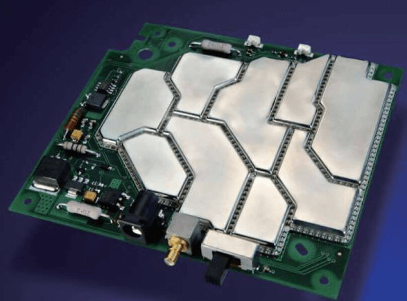
Another essential technique is the implementation of shielding enclosures or cans.
These metal enclosures are placed over sensitive components or entire sections of the PCB to block RF signals from entering or leaving the enclosed area. Shielding enclosures are typically made from materials with high conductivity, such as copper or aluminum, and are designed to provide a continuous conductive path around the shielded area. To ensure optimal performance, it is important to maintain good electrical contact between the enclosure and the PCB ground.
Via stitching is also a valuable method for improving RF shielding on PCBs.
This technique involves placing multiple vias around the perimeter of a shielded area to create a continuous conductive barrier. Vias are small holes drilled through the PCB and filled with conductive material, such as copper, to establish electrical connections between different layers of the board. By stitching vias around the edges of a ground plane or shielding enclosure, designers can enhance the isolation of RF signals and reduce the risk of EMI.
In addition to these techniques, careful layout and routing of signal traces play a critical role in effective RF shielding.
High-frequency signals should be routed away from sensitive components and kept as short as possible to minimize radiation and coupling. Differential signaling, which uses pairs of traces to carry signals with opposite polarities, can also help to reduce EMI by canceling out noise. Furthermore, maintaining adequate spacing between signal traces and ground planes can prevent unwanted coupling and crosstalk.
The use of decoupling capacitors is another important consideration for RF shielding on PCBs.
These capacitors are placed near power supply pins of integrated circuits to filter out high-frequency noise and provide a stable voltage supply. By selecting capacitors with appropriate values and placing them close to the ICs, designers can effectively suppress RF noise and improve overall circuit performance.
Finally, it is essential to consider the materials used in the PCB itself.
High-frequency PCBs often require specialized materials with low dielectric constants and low loss tangents to minimize signal attenuation and dispersion. Materials such as Rogers or Teflon are commonly used in RF applications due to their superior electrical properties. Additionally, the choice of solder mask and surface finish can impact the shielding effectiveness, as certain materials may provide better conductivity and adhesion.
In conclusion, effective RF shielding on PCBs involves a combination of techniques, including the use of ground planes, shielding enclosures, via stitching, careful layout and routing, decoupling capacitors, and appropriate materials. By understanding and implementing these techniques, engineers and designers can ensure the reliable performance of electronic devices in increasingly complex and high-frequency environments.
Materials Used For RF Shielding In PCB Manufacturing
In the realm of printed circuit board (PCB) manufacturing, the importance of radio frequency (RF) shielding cannot be overstated. RF shielding is essential for mitigating electromagnetic interference (EMI) and ensuring the proper functioning of electronic devices. The materials used for RF shielding in PCB manufacturing play a crucial role in achieving effective EMI suppression. Various materials are employed, each with unique properties that make them suitable for specific applications.
One of the most commonly used materials for RF shielding is copper.
Copper is highly conductive, which makes it an excellent choice for creating a barrier against electromagnetic waves. Its effectiveness in shielding is due to its ability to reflect and absorb RF energy, thereby preventing it from interfering with the electronic components on the PCB.
Additionally, copper is relatively easy to work with, allowing for precise fabrication of shielding structures. However, copper is not without its drawbacks; it is prone to oxidation, which can degrade its performance over time. To mitigate this, copper is often coated with other materials such as tin or nickel to enhance its durability and maintain its shielding effectiveness.
Another material frequently used for RF shielding is aluminum.
Aluminum is lightweight and has good conductivity, making it a popular choice for applications where weight is a critical factor. Its ability to form a continuous conductive layer helps in effectively blocking RF signals. Moreover, aluminum is resistant to corrosion, which adds to its longevity as a shielding material. However, aluminum is not as conductive as copper, which can limit its effectiveness in certain high-frequency applications. Despite this, its combination of light weight, corrosion resistance, and adequate shielding properties makes it a valuable material in many PCB designs.
Nickel is another material that finds extensive use in RF shielding.
Nickel’s primary advantage lies in its magnetic properties, which make it particularly effective at shielding against low-frequency electromagnetic interference. This makes nickel an ideal choice for applications where both RF and magnetic shielding are required. Additionally, nickel is often used as a coating material for other metals, such as copper, to enhance their shielding capabilities and protect them from oxidation. The use of nickel in combination with other materials can provide a balanced approach to achieving comprehensive EMI suppression.
In addition to metals, conductive polymers are also gaining traction as RF shielding materials.
These polymers are infused with conductive particles, such as carbon or metal flakes, to create a material that can effectively block RF signals. Conductive polymers offer the advantage of being lightweight and flexible, which allows for innovative PCB designs that are not possible with traditional metal shields. Furthermore, they can be easily applied as coatings or embedded within the PCB layers, providing versatile options for designers. However, the conductivity of these polymers is generally lower than that of metals, which can limit their effectiveness in certain high-frequency applications.
In conclusion, the choice of materials for RF shielding in PCB manufacturing is critical to achieving effective EMI suppression. Copper, aluminum, nickel, and conductive polymers each offer unique advantages and limitations that must be carefully considered based on the specific requirements of the application. By understanding the properties and suitability of these materials, designers can make informed decisions to ensure the optimal performance of their electronic devices. The ongoing advancements in material science continue to expand the possibilities for RF shielding, promising even more effective solutions in the future..
Common Challenges And Solutions In RF Shielding For PCBs
RF shielding on printed circuit boards (PCBs) is a critical aspect of modern electronics design, particularly in applications where electromagnetic interference (EMI) can significantly impact performance.
One of the most common challenges in RF shielding for PCBs is the effective containment of electromagnetic emissions.
These emissions can originate from various components on the PCB, including oscillators, microprocessors, and other high-frequency devices. To mitigate this, designers often employ metal shields or enclosures that cover the sensitive areas of the PCB. However, the implementation of these shields can introduce additional complexities.
Another challenge is the potential for signal degradation due to the introduction of the shield.
While the primary purpose of RF shielding is to prevent unwanted emissions, it can also inadvertently affect the signal integrity of the components it is meant to protect. This is particularly problematic in high-speed digital circuits where even minor signal distortions can lead to significant performance issues. To address this, designers must carefully consider the placement and grounding of the shield. Proper grounding is essential to ensure that the shield effectively attenuates EMI without introducing noise into the system.
Thermal management is another critical issue that arises with RF shielding.
The addition of metal shields can impede airflow and increase the thermal resistance of the PCB, leading to overheating of components. This is especially concerning in high-power applications where efficient heat dissipation is crucial. To overcome this, designers can incorporate thermal vias and heat sinks into the PCB layout. These features help to dissipate heat more effectively, ensuring that the components remain within their operational temperature range.
Moreover, the physical size and weight of the RF shield can pose challenges, particularly in compact and lightweight devices such as smartphones and wearable technology.
The shield must be designed to provide adequate protection without adding excessive bulk or weight. This often requires the use of advanced materials and manufacturing techniques. For instance, designers may opt for lightweight alloys or composite materials that offer high shielding effectiveness while minimizing weight.
Cost is another significant factor in RF shielding for PCBs.
High-quality shielding materials and advanced manufacturing processes can be expensive, which can be a constraint for budget-sensitive projects. To balance cost and performance, designers may need to prioritize the most critical areas for shielding and use cost-effective materials where possible. Additionally, simulation tools can be employed to optimize the design before physical prototypes are made, reducing the need for costly iterations.
In addition to these technical challenges, regulatory compliance is a crucial consideration.
Many countries have stringent regulations regarding EMI emissions, and failure to comply can result in product recalls or fines. Therefore, thorough testing and validation are essential to ensure that the PCB meets all relevant standards. This often involves the use of specialized testing equipment and facilities to measure the effectiveness of the RF shielding.
In conclusion, RF shielding on PCBs presents a range of challenges, from managing electromagnetic emissions and maintaining signal integrity to addressing thermal management and regulatory compliance. By carefully considering these factors and employing a combination of design strategies and advanced materials, designers can effectively mitigate these challenges and ensure the reliable performance of their electronic devices.