Rigid flex pcb fabrication process
Introduction To Rigid Flex PCB Fabrication Process
Rigid-flex PCB fabrication is a sophisticated process that combines the best attributes of both rigid and flexible circuit boards, resulting in a versatile and durable product.
This hybrid technology is increasingly popular in various industries, including aerospace, medical devices, and consumer electronics, due to its ability to meet complex design requirements and enhance performance. Understanding the fabrication process of rigid-flex PCBs is essential for appreciating their advantages and applications.
The fabrication process begins with the design phase, where engineers create a detailed blueprint of the circuit board.
This design must account for the unique properties of both rigid and flexible sections, ensuring that the final product can withstand mechanical stresses and environmental conditions. Advanced software tools are often employed to simulate the performance of the PCB, allowing designers to make necessary adjustments before proceeding to the manufacturing stage.
Once the design is finalized, the next step involves selecting appropriate materials.
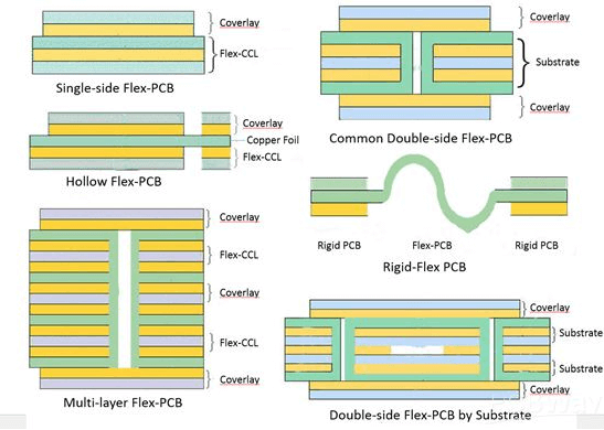
Rigid-flex PCBs typically consist of multiple layers, including rigid substrates made of materials like FR4 and flexible substrates composed of polyimide. These materials are chosen for their excellent electrical properties, thermal stability, and mechanical strength. The combination of rigid and flexible layers allows the PCB to maintain structural integrity while accommodating complex geometries and dynamic movements.
The fabrication process then moves to the lamination stage, where the rigid and flexible layers are bonded together.
This step is crucial for ensuring the mechanical stability and electrical performance of the PCB. The layers are carefully aligned and subjected to high pressure and temperature, causing the adhesive materials to cure and form a strong bond. This lamination process must be meticulously controlled to prevent defects such as delamination or misalignment, which could compromise the functionality of the final product.
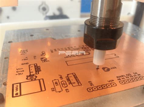
Following lamination, the PCB undergoes drilling and plating processes.
Precision drilling is used to create vias and holes that connect different layers of the circuit board. These holes are then plated with conductive materials, typically copper, to establish electrical connections between the layers. The plating process involves multiple steps, including cleaning, activation, and electroplating, each of which must be carefully monitored to ensure high-quality results.
After drilling and plating, the PCB is subjected to a series of etching processes to define the circuit patterns.
Photolithography techniques are commonly used, where a photosensitive resist is applied to the surface of the PCB and exposed to ultraviolet light through a mask. The exposed areas are then developed, leaving behind a precise pattern that can be etched away using chemical solutions. This process is repeated for each layer of the PCB, resulting in a complex network of conductive traces and pads.
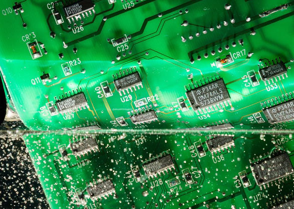
The final stages of rigid-flex PCB fabrication involve assembly and testing.
Components are mounted onto the PCB using surface-mount or through-hole techniques, depending on the design requirements. The assembled PCB is then subjected to rigorous testing to verify its electrical performance and mechanical durability. Automated testing equipment is often used to perform functional tests, ensuring that the PCB meets all specifications and quality standards.
In conclusion, the fabrication of rigid-flex PCBs is a complex and multi-step process that requires careful planning, precise execution, and stringent quality control. By combining the strengths of rigid and flexible circuit boards, rigid-flex PCBs offer unparalleled versatility and reliability, making them an ideal choice for a wide range of applications. Understanding the intricacies of this fabrication process highlights the advanced engineering and manufacturing techniques that contribute to the development of cutting-edge electronic devices.
Key Steps In Rigid Flex PCB Manufacturing
The rigid flex PCB fabrication process is a sophisticated and intricate procedure that combines the best attributes of both rigid and flexible circuit boards. This hybrid technology is increasingly popular in various industries, including aerospace, medical devices, and consumer electronics, due to its ability to provide enhanced design flexibility, reduced weight, and improved reliability. Understanding the key steps in rigid flex PCB manufacturing is essential for appreciating the complexity and precision involved in creating these advanced electronic components.
To begin with, the design phase is crucial in the rigid flex PCB fabrication process.
Engineers and designers use specialized software to create detailed schematics and layouts that meet the specific requirements of the application. This phase involves careful consideration of factors such as signal integrity, thermal management, and mechanical stability. Once the design is finalized, it is converted into a format suitable for manufacturing, typically Gerber files, which contain all the necessary information for the subsequent steps.
Following the design phase, the next step is the selection of materials.
Rigid flex PCBs are composed of a combination of rigid and flexible substrates, typically FR4 for the rigid sections and polyimide for the flexible sections. These materials are chosen for their excellent electrical, thermal, and mechanical properties. The selection process also involves determining the appropriate thickness and copper weight for each layer, which are critical for ensuring the board’s performance and durability.
Once the materials are selected, the fabrication process begins with the creation of the individual layers.
This involves laminating the copper-clad substrates with photoresist, a light-sensitive material that allows for the precise transfer of the circuit pattern onto the copper surface. The photoresist-coated substrates are then exposed to ultraviolet light through a photomask, which defines the circuit pattern. The exposed areas of the photoresist harden, while the unexposed areas remain soft and can be washed away, leaving behind the desired circuit pattern on the copper surface.
The next step is etching, where the unwanted copper is removed from the substrate, leaving only the circuit traces defined by the hardened photoresist.
This is typically done using a chemical etchant, such as ferric chloride or ammonium persulfate. After etching, the remaining photoresist is stripped away, revealing the completed circuit pattern on each layer.
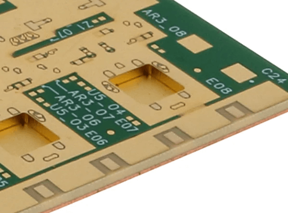
Following the etching process, the individual layers are aligned and laminated together to form a single, cohesive board.
This involves stacking the layers in the correct order and applying heat and pressure to bond them together. For rigid flex PCBs, this step also includes the integration of the flexible sections, which are carefully positioned to ensure proper alignment and functionality.
Once the layers are laminated, the next step is drilling, where holes are created for vias, through-hole components, and mounting points.
This is typically done using precision drilling machines equipped with carbide or diamond-coated drill bits. The drilled holes are then plated with copper to create electrical connections between the different layers of the board.
The final steps in the rigid flex PCB fabrication process include solder mask application, surface finish, and assembly.
The solder mask is a protective layer applied to the surface of the board to prevent solder bridges and short circuits during assembly. The surface finish, such as HASL, ENIG, or OSP, is applied to the exposed copper pads to enhance solderability and protect against oxidation. Finally, the board is assembled with components using techniques such as surface mount technology (SMT) or through-hole technology (THT), depending on the design requirements.
In conclusion, the rigid flex PCB fabrication process involves a series of meticulously executed steps, each critical to the overall performance and reliability of the final product. From design and material selection to layer creation, etching, lamination, drilling, and assembly, every phase requires precision and expertise to ensure the successful production of these advanced electronic components.
Advantages Of Rigid Flex PCBs In Modern Electronics
Rigid flex PCBs, a hybrid of rigid and flexible circuit boards, have become increasingly popular in modern electronics due to their unique advantages. These circuit boards combine the best features of both rigid and flexible PCBs, offering a versatile solution for a wide range of applications.
One of the primary benefits of rigid flex PCBs is their ability to save space and reduce weight.
By integrating flexible circuits with rigid boards, designers can create more compact and lightweight devices, which is particularly important in industries such as aerospace, medical devices, and consumer electronics where space and weight are critical factors.
Moreover, rigid flex PCBs provide enhanced reliability and durability.
The flexible sections of these boards can withstand bending and flexing, which reduces the risk of damage and failure in applications where movement or vibration is common. This makes them ideal for use in wearable technology, automotive electronics, and other environments where traditional rigid PCBs might fail. Additionally, the seamless integration of rigid and flexible sections eliminates the need for connectors and cables, which are often points of failure in electronic devices. This not only improves the overall reliability of the device but also simplifies the assembly process, reducing manufacturing costs and time.
Another significant advantage of rigid flex PCBs is their ability to improve signal integrity.
The flexible sections of these boards can be designed to minimize signal interference and crosstalk, which is crucial for high-speed and high-frequency applications. This makes rigid flex PCBs an excellent choice for advanced communication systems, military electronics, and other applications where signal integrity is paramount. Furthermore, the ability to design complex three-dimensional shapes with rigid flex PCBs allows for more efficient use of space within a device, enabling the creation of more sophisticated and compact electronic products.
In addition to these technical benefits, rigid flex PCBs also offer environmental advantages.
The reduction in the number of connectors and cables not only decreases the overall material usage but also reduces the environmental impact associated with the production and disposal of these components. Moreover, the increased reliability and durability of rigid flex PCBs can lead to longer product lifespans, which in turn reduces electronic waste. This aligns with the growing emphasis on sustainability and environmental responsibility in the electronics industry.
The versatility of rigid flex PCBs also extends to their design and manufacturing processes.
Designers have greater freedom to create innovative and complex layouts that would be difficult or impossible to achieve with traditional rigid or flexible PCBs alone. This flexibility in design can lead to the development of new and improved electronic devices that push the boundaries of what is currently possible. Additionally, the ability to prototype and test rigid flex PCBs quickly and efficiently allows for faster development cycles and a more agile approach to product development.
In conclusion, the advantages of rigid flex PCBs in modern electronics are numerous and significant. Their ability to save space and reduce weight, enhance reliability and durability, improve signal integrity, and offer environmental benefits make them an attractive option for a wide range of applications. As technology continues to advance and the demand for more compact, reliable, and sophisticated electronic devices grows, the adoption of rigid flex PCBs is likely to increase, further solidifying their importance in the future of electronics.
Common Challenges In Rigid Flex PCB Fabrication And Solutions
Rigid flex PCB fabrication is a sophisticated process that combines the benefits of both rigid and flexible circuit boards, offering enhanced design versatility and improved performance in complex electronic applications. However, this intricate process is not without its challenges. Understanding these common challenges and their solutions is crucial for achieving optimal results in rigid flex PCB fabrication.
One of the primary challenges in rigid flex PCB fabrication is the precise alignment of the rigid and flexible layers.
Misalignment can lead to electrical failures and mechanical stress, compromising the integrity of the final product. To address this issue, manufacturers employ advanced alignment techniques and equipment, such as optical alignment systems, which ensure that each layer is accurately positioned. Additionally, implementing stringent quality control measures throughout the fabrication process can help detect and correct alignment issues early on.
Another significant challenge is the management of different material properties.
Rigid and flexible materials have distinct thermal expansion coefficients, which can cause warping or delamination during the fabrication process. To mitigate this, manufacturers carefully select materials with compatible thermal properties and use controlled lamination processes to minimize stress. Furthermore, conducting thorough thermal analysis and simulations can help predict and address potential issues before they arise.
The complexity of the design itself can also pose challenges.
Rigid flex PCBs often require intricate routing and precise placement of components, which can be difficult to achieve without advanced design software and expertise. To overcome this, designers use specialized CAD tools that support rigid flex PCB design, allowing for accurate modeling and simulation of the final product. Collaboration between designers and manufacturers is also essential to ensure that the design is feasible and can be efficiently fabricated.
Manufacturing yield is another area of concern in rigid flex PCB fabrication.
The combination of rigid and flexible sections can lead to higher defect rates, particularly in the transition areas where the two materials meet. To improve yield, manufacturers implement robust testing and inspection protocols, such as automated optical inspection (AOI) and X-ray inspection, to identify and rectify defects early in the process. Additionally, continuous process optimization and employee training can help reduce the occurrence of defects and improve overall yield.
Cost management is a further challenge in rigid flex PCB fabrication.
The complexity of the process and the need for specialized materials and equipment can drive up production costs. To address this, manufacturers focus on optimizing their processes to reduce waste and improve efficiency. This includes adopting lean manufacturing principles, investing in advanced automation technologies, and sourcing materials from reliable suppliers to ensure consistent quality and cost-effectiveness.
Finally, ensuring reliability and durability in the final product is paramount.
Rigid flex PCBs are often used in demanding applications where failure is not an option. To ensure reliability, manufacturers conduct rigorous testing, including thermal cycling, mechanical stress testing, and environmental testing, to validate the performance of the PCBs under various conditions. Implementing a comprehensive reliability testing program helps identify potential weaknesses and allows for corrective actions to be taken before the product reaches the market.
In conclusion, while rigid flex PCB fabrication presents several challenges, these can be effectively managed through a combination of advanced technology, meticulous planning, and continuous improvement. By addressing issues related to alignment, material properties, design complexity, manufacturing yield, cost management, and reliability, manufacturers can produce high-quality rigid flex PCBs that meet the demanding requirements of modern electronic applications.