Rigid-Flex PCB Fabrication: Processes, Materials, and Applications
Introduction to Rigid-Flex PCB Technology
Rigid-flex printed circuit boards (PCBs) represent a revolutionary advancement in electronic interconnection technology, combining the best attributes of both rigid and flexible circuit boards. This hybrid construction offers numerous advantages over traditional PCB solutions, enabling innovative product designs across multiple industries.
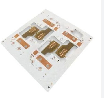
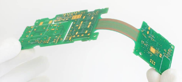
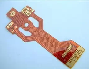
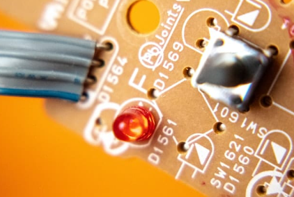
Rigid-flex PCBs integrate rigid board substrates with flexible circuitry, allowing three-dimensional packaging configurations that would be impossible with conventional PCBs. The technology eliminates the need for connectors and cables between rigid boards, reducing points of failure while improving reliability and signal integrity. These characteristics make rigid-flex PCBs particularly valuable in applications where space constraints, weight reduction, and reliability are critical factors.
The global rigid-flex PCB market has experienced significant growth in recent years, driven by increasing demand from aerospace, medical devices, consumer electronics, and automotive sectors. According to market research, the rigid-flex PCB industry is projected to continue its expansion as more product designers recognize the benefits of this technology.
Materials Used in Rigid-Flex PCB Fabrication
The performance and reliability of rigid-flex PCBs depend heavily on the materials selected for their construction. Manufacturers must carefully choose materials that meet electrical, mechanical, and thermal requirements while ensuring compatibility between rigid and flexible sections.
Base Materials
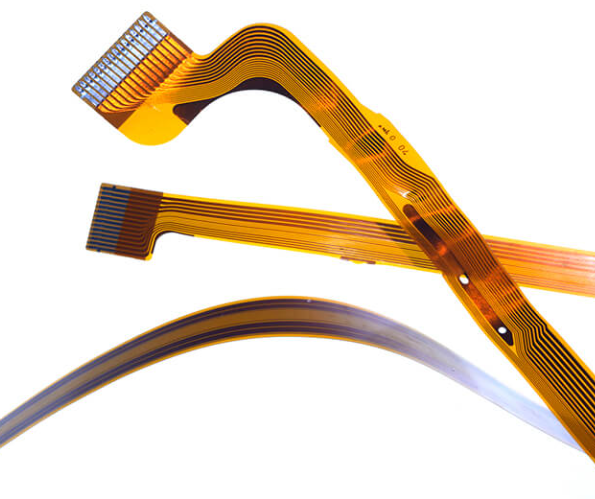
The flexible portions typically use polyimide films as the base material, with common thicknesses ranging from 12.5 to 50 microns. Polyimide offers excellent thermal stability (withstanding temperatures up to 400°C), good dielectric properties, and mechanical flexibility. DuPont’s Kapton is the most well-known polyimide film, though other manufacturers provide comparable alternatives.
For rigid sections, standard FR-4 epoxy-glass laminates are most common, though high-frequency applications may use specialized materials like Rogers or Taconic substrates. The key consideration is matching the thermal expansion characteristics between rigid and flexible materials to prevent delamination or cracking during thermal cycling.
Conductive Materials
Copper remains the primary conductor for both rigid and flexible circuits. Flexible circuits typically use rolled annealed copper rather than electrodeposited copper due to its better fatigue resistance during flexing. Thicknesses generally range from 12 to 35 microns (⅓ oz to 1 oz), with thinner copper providing greater flexibility.
Adhesives and Bonding Materials
Acrylic or epoxy-based adhesives bond the layers together in rigid-flex constructions. Newer adhesiveless laminates are gaining popularity as they offer improved thermal performance and thinner profiles. These materials incorporate a proprietary bonding layer that activates under heat and pressure without requiring separate adhesive films.
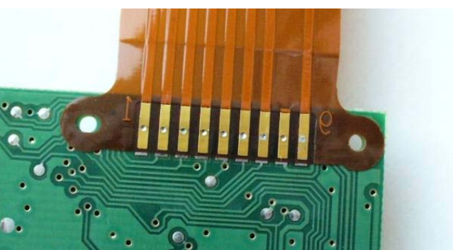
Coverlay and Solder Mask
Flexible circuits use polyimide coverlay instead of solder mask for insulation and protection. The coverlay is precision-cut to expose pads and features adhesive on one side for lamination. In rigid sections, conventional liquid photoimageable solder mask (LPISM) is typically applied.
Rigid-Flex PCB Fabrication Process
The manufacturing process for rigid-flex PCBs is considerably more complex than for standard rigid boards, requiring specialized equipment and expertise. The following steps outline the typical fabrication workflow:
1. Material Preparation and Cutting
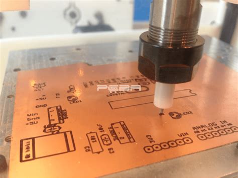
The process begins with cutting the flexible and rigid materials to size. Cleanroom conditions are essential to prevent contamination that could affect adhesion or cause electrical faults. Manufacturers often use laser cutting for precision, especially for prototype quantities.
2. Drilling and Via Formation
Mechanical drilling creates through-holes and vias in both rigid and flexible sections. For high-density interconnects (HDI) designs, laser drilling may be employed to create microvias smaller than 100 microns in diameter. Sequential lamination may be required for multilayer constructions with buried or blind vias.
3. Circuit Patterning
Photolithographic processes transfer the circuit patterns onto the copper layers. This typically involves:
- Cleaning and surface preparation
- Application of photoresist (dry film or liquid)
- Exposure through phototool or direct imaging
- Development to remove unexposed resist
- Etching to remove unwanted copper
- Stripping remaining resist
Advanced facilities may use pattern plating (additive) processes instead of subtractive etching for finer features.
4. Coverlay Application (Flexible Sections)
The polyimide coverlay is precisely aligned over the flexible circuits and laminated using heat and pressure. Laser or die cutting opens windows in the coverlay for component mounting and interconnection points.
5. Layer Alignment and Lamination
Operators carefully stack the rigid and flexible layers according to the design, ensuring proper alignment of all features. The stack-up then undergoes controlled thermal lamination to bond the layers into a unified structure. This critical step requires precise control of temperature, pressure, and vacuum to prevent voids or delamination.
6. Surface Finishing
Exposed copper surfaces receive finishing treatments to protect against oxidation and enhance solderability. Common options include:
- Electroless nickel immersion gold (ENIG)
- Immersion silver
- Organic solderability preservative (OSP)
- Electrolytic hard gold (for contact surfaces)
7. Electrical Testing and Inspection
Automated optical inspection (AOI) checks for physical defects, while electrical testing verifies continuity and isolation according to the netlist. Flying probe or fixture-based testing may be employed depending on production volume and complexity.
8. Routing and Singulation
Final board outlines are cut using precision routing equipment. Some designs may require additional milling operations to create complex shapes or relieve bending stress in transition areas between rigid and flexible sections.
9. Final Quality Assurance
Completed boards undergo thorough visual inspection and may be subjected to additional reliability testing such as thermal cycling or bend testing, particularly for prototypes or mission-critical applications.
Design Considerations for Rigid-Flex PCBs
Successful rigid-flex PCB implementation requires careful attention to design factors that differ from conventional PCB layouts:
Bend Radius and Flex Life
The minimum bend radius is typically 6-10 times the total thickness of the flexible section. Tighter radii risk damaging conductors. Dynamic flex applications (continuous movement) require more conservative design rules than static flex (bent only during installation).
Transition Zones
Areas where rigid and flexible materials meet represent critical stress points. Designers should avoid placing vias or components near these transitions and may incorporate strain relief features like tapered sections or additional stiffeners.
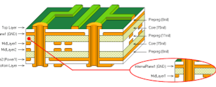
Layer Stack-up Planning
Proper material selection and layer sequencing are essential for achieving both flexibility where needed and rigidity where required. Symmetrical constructions help prevent warping, while proper copper balancing maintains dimensional stability.
Routing Considerations
Conductors in flexible areas should:
- Run perpendicular to the bend axis when possible
- Use curved traces instead of sharp angles
- Incorporate teardrops at pad connections
- Avoid abrupt width changes that create stress concentrations
Component Placement
Surface-mount devices should generally be placed only on rigid sections unless specifically designed for flexible mounting. Any components on flex areas require additional support and strain relief.
Applications of Rigid-Flex PCBs
The unique capabilities of rigid-flex PCBs have enabled their adoption across diverse industries:
Aerospace and Defense
Avionics systems benefit from rigid-flex PCBs’ vibration resistance, light weight, and reliability in extreme environments. Applications include flight control systems, satellite components, and military communications equipment.
Medical Devices
Medical electronics increasingly use rigid-flex technology for portable diagnostic equipment, implantable devices, and surgical instruments where reliability and compact packaging are critical.
Consumer Electronics
Smartphones, wearables, and digital cameras employ rigid-flex PCBs to achieve sleek form factors while maintaining durability. The technology enables innovative folding and sliding designs in mobile devices.
Automotive Systems
Advanced driver assistance systems (ADAS), infotainment consoles, and engine control units utilize rigid-flex PCBs to withstand automotive vibration and temperature extremes while reducing weight and complexity.
Industrial Equipment
Robotics, automation systems, and instrumentation benefit from rigid-flex solutions that reduce interconnection points while withstanding harsh industrial environments.
Advantages of Rigid-Flex PCB Technology
The growing adoption of rigid-flex PCBs stems from several compelling advantages:
Reliability Enhancement
By eliminating connectors and discrete wiring between board sections, rigid-flex PCBs remove common failure points. The monolithic construction improves resistance to vibration and mechanical stress.
Space and Weight Reduction
Rigid-flex designs often enable 30-50% space savings compared to traditional multi-board assemblies with connectors. The weight reduction is particularly valuable in aerospace and portable applications.
Improved Signal Integrity
High-speed signals benefit from continuous impedance control without the discontinuities introduced by connectors. This becomes increasingly important for high-frequency RF and digital circuits.
Simplified Assembly
Rigid-flex PCBs reduce the number of components in the final assembly by eliminating connectors and cables. This simplifies manufacturing while improving yield and reliability.
Design Flexibility
Engineers can create three-dimensional packaging solutions that would be impractical or impossible with conventional PCBs, enabling innovative product architectures.
Challenges in Rigid-Flex PCB Fabrication
Despite their advantages, rigid-flex PCBs present several manufacturing challenges:
Higher Initial Costs
Rigid-flex PCBs typically cost 3-5 times more than equivalent rigid boards due to specialized materials, additional processing steps, and lower production volumes. However, the total system cost may be lower when considering reduced assembly time and improved reliability.
Complex Design Requirements
Designing rigid-flex circuits requires expertise in both rigid and flexible PCB technologies, along with understanding of mechanical stress factors. Many designers require specialized training or collaboration with fabrication experts.
Limited Supplier Base
The specialized nature of rigid-flex manufacturing means fewer qualified suppliers compared to conventional PCBs. Lead times may be longer, particularly for complex designs.
Testing Difficulties
The three-dimensional nature of rigid-flex assemblies can complicate testing, requiring custom fixtures or specialized equipment for thorough validation.
Future Trends in Rigid-Flex PCB Technology
Several emerging trends are shaping the future of rigid-flex PCB fabrication:
Ultra-Thin Constructions
Advancements in materials and processing enable thinner rigid-flex boards for applications like wearable electronics and implantable medical devices. Adhesiveless laminates and ultra-thin dielectrics facilitate this trend.
High-Density Interconnect (HDI)
Increasing component density drives adoption of HDI technologies in rigid-flex PCBs, including microvias, fine-pitch traces, and advanced packaging techniques like package-on-package (PoP).
Embedded Components
Passive components and even some active devices are being embedded within rigid-flex structures to save space and improve performance. This requires close collaboration between designers and fabricators.
3D Printing Additive Processes
Emerging additive manufacturing techniques may complement traditional rigid-flex fabrication, particularly for prototyping and low-volume production. Printed electronics could enable new flexible circuit capabilities.
Sustainable Materials
Environmental considerations are driving development of halogen-free and recyclable materials for rigid-flex applications without compromising performance.
Conclusion
Rigid-flex PCB fabrication represents a sophisticated merging of rigid and flexible circuit technologies, offering unparalleled design freedom and reliability advantages for modern electronic products. While the manufacturing process is complex and requires specialized expertise, the benefits in terms of space savings, weight reduction, and improved performance continue to drive adoption across multiple industries.
As materials and processes advance, rigid-flex technology will likely play an increasingly important role in electronics packaging, particularly for applications demanding miniaturization, durability, and three-dimensional configurations. Designers and manufacturers who master rigid-flex PCB fabrication will be well-positioned to create the next generation of innovative electronic products.
Successful implementation requires close collaboration between design engineers and fabrication specialists from the earliest stages of product development. By understanding both the capabilities and limitations of rigid-flex technology, teams can fully leverage its potential while avoiding common pitfalls. With proper design and manufacturing execution, rigid-flex PCBs provide reliable, high-performance solutions for even the most challenging electronic packaging requirements.